Cart ( )
2N5551 Circuit Diagram Description Transistor 2N5551 Project
2024/10/19 15:24:42
Views:
The 2N5551 is a high-voltage NPN type transistor that is primarily used in general-purpose enhancement circuits.Due to its robust design,it is widely used in applications that require the ability to handle high voltage and DC current.Its characteristics make it suitable for high-speed switches in low power circuits, and can also be used in various electronic projects.In this article, we will explore the characteristics of the 2N5551 transistor, including a detailed explanation of the 2N5551 circuit diagram.
Cek Transistor 2n5551 / 2n5451
Table of Contents
- What is the 2N5551 Transistor?
- 2N5551 Voltage Ratings
- 2N5551 Circuit Diagram Overview
- 2N5551 Equivalent Transistors
- 2N5551 Datasheet
- Conclusion
- Commonly Asked Questions
What is the 2N5551 Transistor?
The 2N5551 is an NPN type bipolar junction transistor (BJT) used for general-purpose switching and amplification tasks.It is suitable for high voltage applications up to 160V, making it ideal for circuits operating in such conditions.The transistor has a DC current rating of 600mA, making it sufficient for use in low-power amplification circuits.
2N5551 Pinout

In order to successfully use the 2N5551 transistor in the project, it's important to understand its pin arrangement.The pin diagram of the 2N5551 consists of three main terminals: the emitter, base, and collector.
This straightforward pinout configuration is common in NPN transistors and ensures ease of integration into various circuits.
2N5551 Voltage Ratings
When designing the circuit, it is vital to consider the voltage rating of 2N5551 to avoid component damage.The 2N5551 has a maximum collector-emitter voltage of 160V, which allows it to handle high-voltage applications beyond the limits of other transistors.It is also capable of managing collector currents up to 600mA, making it useful in circuits that require direct power switching.
To ensure safe operation, the applied voltage must be kept within these ratings.Exceeding the maximum voltage or current values could damage the transistor and lead to failure.
2N5551 Circuit Diagram Overview
2N5551 Circuit Diagram Overview
This is a circuit diagram containing 2N5551 NPN transistors, which may operate as an oscillator or amplifier circuit, depending on its arrangement.
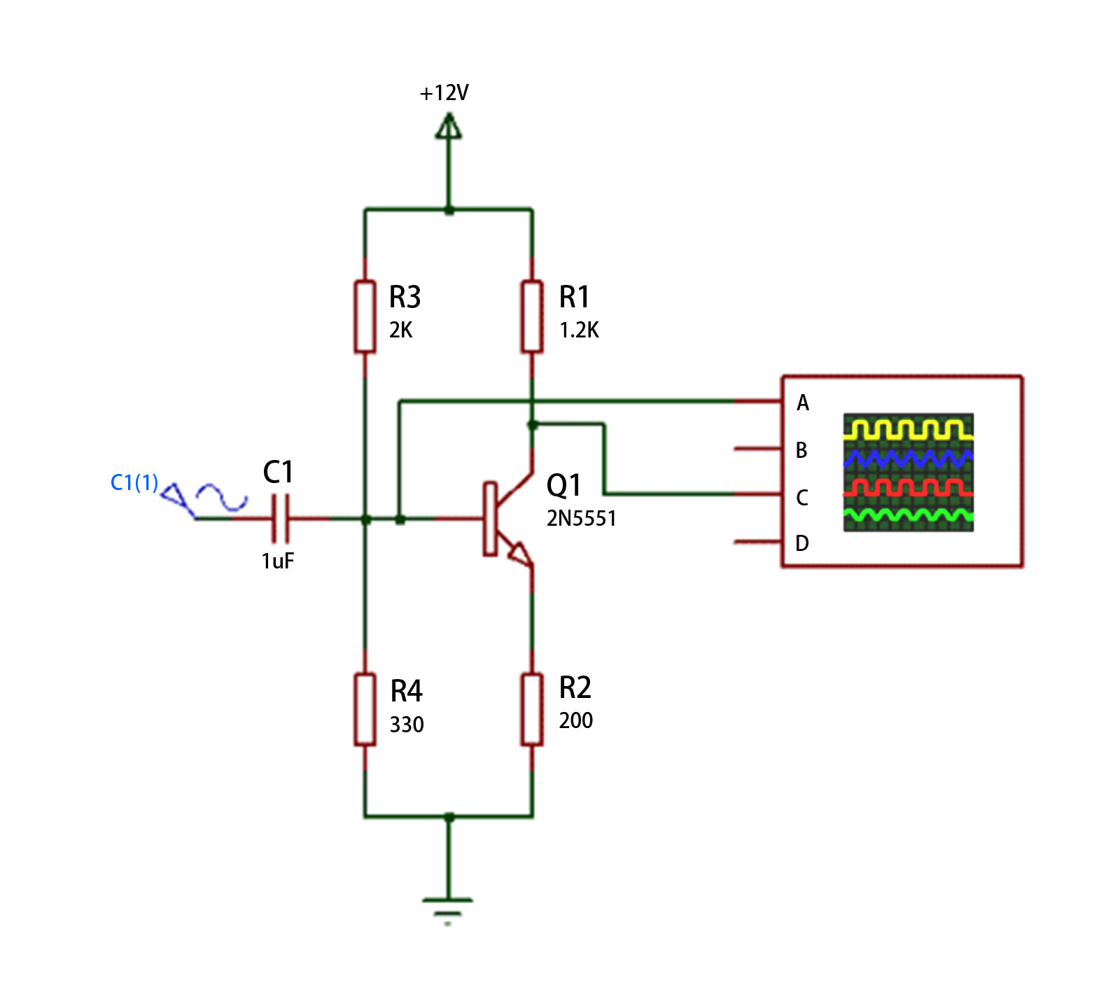
Multi-stage amplifier
This circuit is a multistage amplifiers,especially cascaded or common-base amplifiers.It uses numerous transistors to amplify the signal in numerous stages, thereby increasing overall gain and performance.
Push-pull transistor drive circuit
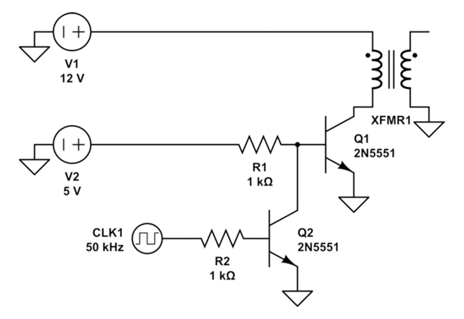
This is usually a push-pull transistor driver circuit, often used in DC-DC converters or power supplies.The circuit uses two 2N5551 NPN transistors (Q1 and Q2) to drive the primary winding of the transformer (XFMR1) and switch the power supply at a high frequency.
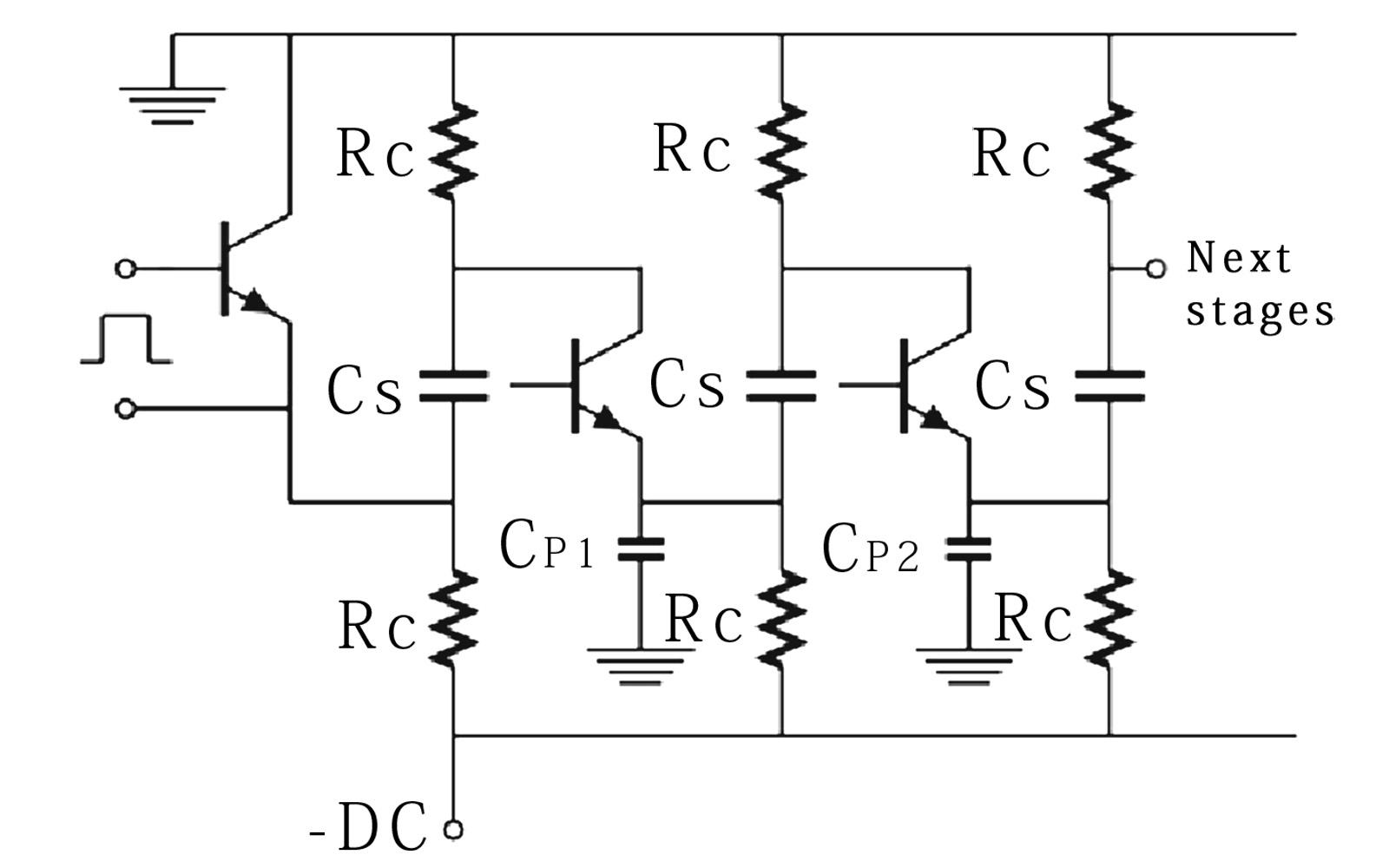
Pulse amplifier circuit

This is a pulse amplifier circuit using 2N5551 NPN transistors designed to amplify input pulses.The circuit is designed to handle high-frequency input pulses, with very short rise and fall times (≤10 ns), and a duty cycle of 1.0%.
2N5551 Equivalent Transistors
Several transistors have similar characteristics to the 2N5551 and can be used as replacements in circuits.Here are some of the 2N5551 equivalent transistors include:
Choosing the appropriate equivalent transistor depends on the specific requirements of the circuit, such as the voltage and current requirements.
2N5551 Complementary Transistor
In circuits that require NPN and PNP transistors, it's common to use complementary transistor pairs to achieve balanced operation. The 2n5551 complementary PNP transistor is the 2N5401.The two transistors are often paired in amplifier designs or push-pull configurations to handle positive and negative signal swings.
The pairing of 2N5551 and 2N5401 makes high-voltage amplifiers and switches possible, offering designers more flexibility when building complex circuits.
2N5551 Datasheet
When designing a circuit using 2N5551, it is very important to look at the 2N5551 data sheet.The data sheet provides all the necessary electrical characteristics, including maximum voltage, current rating, conversion frequency and other vital parameters.
Conclusion
Whether you're designing audio amplifiers, high-speed switches, or relay drivers, the 2N5551 is a great choice.Always consult the 2N5551 data sheet for detailed specifications and consider its complementary and equivalent transistors as required by the project.
Commonly Asked Questions
What is the 2N5551 transistor utilized for in a push-pull circuit?
It drives the stack effectively, working with a PNP partner like 2N5401 to intensify positive and negative flag parts.Why utilize 2N5551 in an oscillator circuit?
Its tall voltage capacity and 100MHz move recurrence make it perfect for high-frequency oscillators, guaranteeing soundness.Can 2N5551 be utilized in sound enhancers?
Yes, it's appropriate for low-power sound enhancement due to its tall pick up and moo commotion.What are key voltage appraisals of 2N5551?
Vceo: 160V, Vcbo: 180V, and Vebo: 6V-suitable for high-voltage applications.What are common 2N5551 applications?
Utilized in high-voltage intensifiers, beat intensifiers, push-pull circuits, and RF enhancers.Related Information

-

-
Phone
+86 135 3401 3447 -
Whatsapp