 Cart ( )
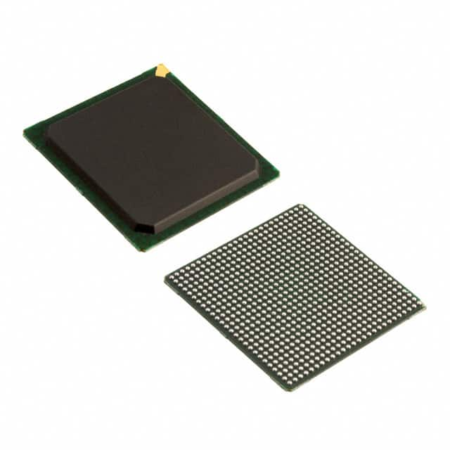
lmages are for reference only See Product Specifications

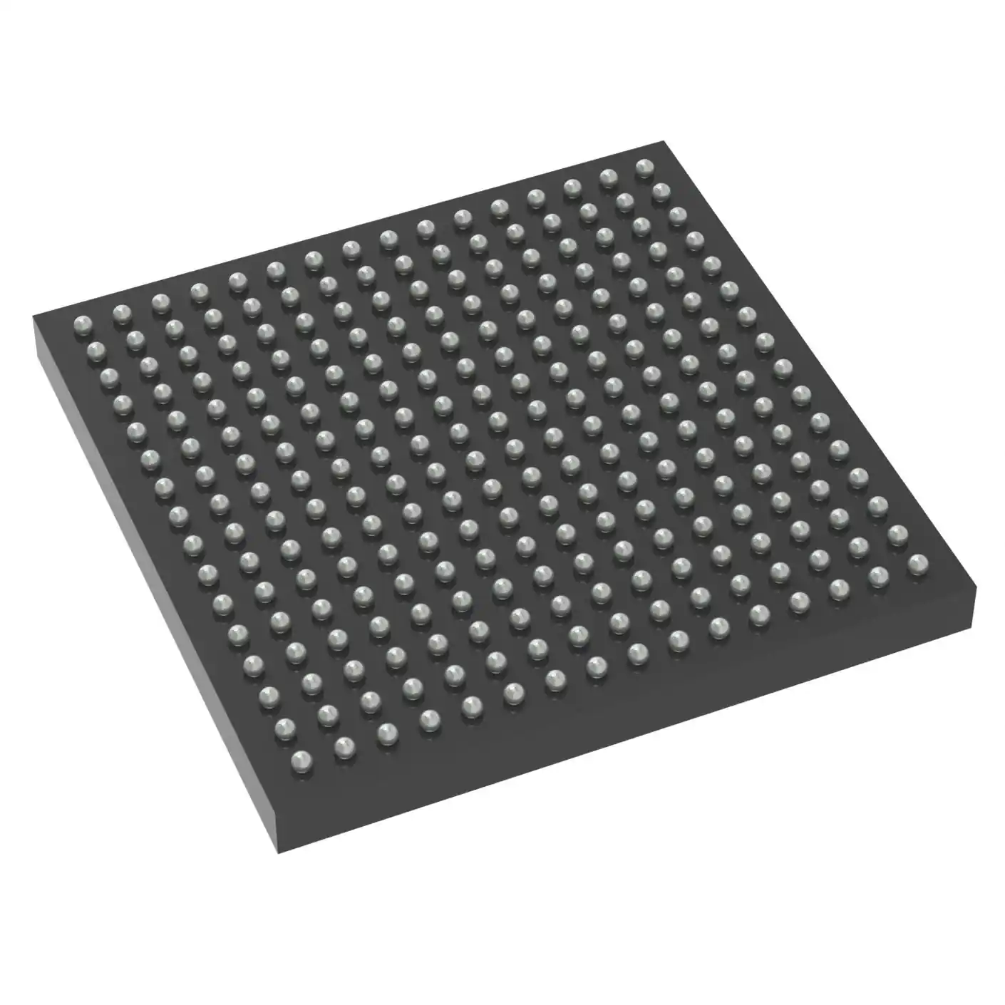
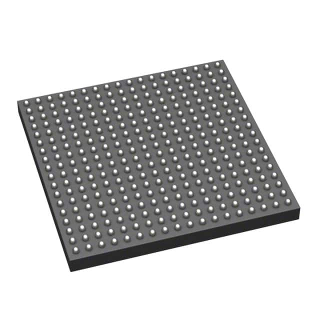
AMD Xilinx XC6SLX45-2FGG676I

- Part No.:
- XC6SLX45-2FGG676I
- Manufacturer:
- AMD Xilinx
- Package:
- 676-BGA
- Datasheet:
-
 XC6SLX45-2FGG676I.pdf

- Description:
- IC FPGA 358 I/O 676FBGA
- In Stock:
- 2748
- Quantity:
- Add To Cart
- For more detailed including pricing and shipping


- Quick response, quick quotation

- Flash shipment, no worries after sales

- Original channel, guarantee of the authentic products
Please send RFQ , we will respond immediately.
 Purchase and inquiry
XC6SLX45-2FGG676I Specifications
- Package/Case:676-BGA
- Packaging:Tray
- Series:Spartan®-6 LX
- ProductStatus:Active
- NumberofLABs/CLBs:3411
- NumberofLogicElements/Cells:43661
- TotalRAMBits:2138112
- NumberofI/O:358
- NumberofGates:-
- Voltage-Supply:1.14V ~ 1.26V
- MountingType:Surface Mount
- OperatingTemperature:-40°C ~ 100°C (TJ)
XC6SLX45-2FGG676I this integrated circuit is available in factory sealed anti static packs. at icwhale.com. Please read product page below detail information. including XC6SLX45-2FGG676I price, data-sheet, in-stock availability, technical difficulties. Also. Quickly Enter the access of compare listing to find out replaceable electronic parts. If you want to retrieve comprehensive data for XC6SLX45-2FGG676I to optimize the supply chain (including cross references, life-cycle, parametric, counterfeit risk, obsolescence managements forecasts), please contact to our Tech-supports team.
Purchase in icwhale.com
There is no doubt that you may place an order without registering to icwhale.com.
We strongly suggest you sign in our shop before purchasing as you can track your order real-time tracking.
Means of Payment in icwhale.com
For your convenience, we support multiple payment methods in USD, including PayPal, Credit Card, wire transfer. and Alipay.
RFQ (Request for Quotations) in icwhale.com
It is recommended to acquire for quotations to get the latest prices and inventories about the parts.
Our sales will reply to your request by email within 24 hours.
Warm reminder
1. You'll receive an order information email in your email inbox. (Please remember to check the spam folder if you didn't hear from us).
2. Since inventories and prices may fluctuate to some extent, the sales manager is going to reconfirm the order and let you know if there are any updates.
Shipping & Handling
Shipping fee starts at $35, but some countries will exceed $35. For example (South Africa, Brazil, India, Pakistan, Israel, etc.)
The basic freight (for package ≤0.5kg or corresponding volume) depends on the time zone and countries.
Shipping Method
Currently, our products are shipped through DHL, FedEx, SF, UPS and China Post.
Order Tracking for International Orders
Once your order has been shipped, the tracking number will be sent to the email address registered to your account. This information can also be viewed when logged into your account in the "my account" page.
 XC6SLX45-2FGG676I information
Views:
XC6SLX45-2FGG676I Typical application Circuitry
The XC6SLX45-2FGG676I is an FPGA from the Xilinx Spartan-6 family. This FPGA offers a wide range of versatile features making it suitable for various applications, including communications, automotive, and video processing. It has 45,000 logic cells, 676 pins in a FGG package, and offers features such as memory controllers, DSP slices, and high-speed transceivers. Below is a detailed guide to connect the XC6SLX45-2FGG676I FPGA:
1. Power Supply: Connect the VCCINT pins (e.g., Pin A22, Pin C13) to a 1.2V power supply, which serves as the core voltage for the XC6SLX45-2FGG676I. The VCCAUX pins (e.g., Pin R3, Pin T4) should be connected to a 2.5V or 3.3V supply. For I/O voltage, connect the VCCO pins (e.g., Pin L12, Pin F8) to a voltage level matching your I/O standard. To lessen power supply noise, use decoupling capacitors next to these pins.
2. Grounding: Connect all GND pins (e.g., Pin K3, Pin A9) to the system ground. Proper grounding is vital for stable FPGA operation.
3. Clock Inputs: Connect your primary system clock to the global clock input pins (GCLK), such as GCLK0 (Pin V10). The XC6SLX45-2FGG676I FPGA has dedicated clock management resources, including PLLs and clock buffers.
4. JTAG Interface: To program and debug the FPGA, connect a JTAG programmer to the TDI (Pin P6), TDO (Pin P7), TMS (Pin N5), and TCK (Pin N6) pins. Connect the TDO of the programmer to the TDI of the FPGA and the TDI of the programmer to the TDO of the FPGA. Also, connect the TMS and TCK pins accordingly.
5. Configuration Memory: To configure the XC6SLX45-2FGG676I, use an external SPI flash memory. Connect the SPI_CLK (Pin R11), SPI_MOSI (Pin R10), SPI_MISO (Pin R9), and SPI_SS (Pin T10) pins to the corresponding pins on the SPI flash memory.
6. User I/O: The FPGA has a large number of I/O pins that can be connected to various components such as sensors, actuators, and communication interfaces. Connect the I/O pins to the respective signals in your system based on your design requirements.
7. Differential Pairs: For differential signal interfaces like LVDS, connect the positive and negative signal pairs to the appropriate I/O pins.
8. Reset: Connect the dedicated PROGRAM_B pin (Pin U16) to an external reset switch or microcontroller GPIO pin to initiate a configuration reset.
9. Bank Voltages: The I/O pins are organized into banks. Each bank can support different I/O standards. Connect the VCCO pins of each bank to the required voltage level for your specific I/O standard.
10. Startup Sequence: Follow the recommended power-up sequence in the XC6SLX45-2FGG676I datasheet. Generally, VCCINT should be powered first, followed by VCCAUX and VCCO.
11. Thermal Management: Since the XC6SLX45-2FGG676I can generate heat during operation, consider using a heat sink or proper ventilation to ensure optimal thermal performance.
To summarize, when connecting the XC6SLX45-2FGG676I FPGA, pay careful attention to power supplies, grounding, clock inputs, JTAG interface, configuration memory, user I/O, differential pairs, reset, bank voltages, startup sequence, and thermal management. Proper connection is crucial for achieving reliable and optimal performance in your designs. For further in-depth details and suggestions, see to the XC6SLX45-2FGG676I datasheet and user manual.
XC6SLX45-2FGG676I FAQ
1. How to order XC6SLX45-2FGG676I on icwhale.com?
Currently, icwhale.com only provide peer-to-peer order processing. While you submit the RFQ, our professional agent will contact you with the competitive prices in the global market, and our agent will prompt you to finish the order if you accept our offers.
2. How does icwhale.com guarantee that XC6SLX45-2FGG676I is from the original manufacturer or authorized agents?
We have a professional and experienced quality control team to strictly verify and test the XC6SLX45-2FGG676I. All suppliers must pass our qualification reviews before they can publish their products including XC6SLX45-2FGG676I on icwhale.com; we pay more attention to the channels and quality of XC6SLX45-2FGG676I products than any other customer. We strictly implement supplier audits, so you can purchase with confidence.
3. Are the XC6SLX45-2FGG676I price and inventory displayed accurate?
The price and inventory of XC6SLX45-2FGG676I fluctuates frequently and cannot be updated in time, it will be updated periodically within 24 hours. And, our quotation usually expires after 5 days.
4. What forms of payment are accepted?
Wire Transfer, PayPal, Alipay, Wechat, Credit Card, Western Union, MoneyGram, and Escrow are all acceptable.
Warm Tips: Some orders in certain payment forms may require handling fee.
5. How is the shipping arranged?
Customers can choose industry-leading freight companies, including DHL, UPS, FedEx, TNT, and Registered Mail. Shipping insurance is also available.
Once your order has been processed for shipment, our salesperson will send you an email advising you of the shipping status and tracking number.
Warm Tips: It may take up to 24 hours for the carriers to display tracking information. Usually, express delivery takes 3-5 days, and registered mail takes 25-60 days.
6. What is the process for return or replacement of XC6SLX45-2FGG676I?
All goods will implement Pre-Shipment Inspection (PSI), selected at random from all batches of your order to do a systematic inspection before arranging the shipment. If there is something wrong with the XC6SLX45-2FGG676I we delivered, we will accept the replacement or return of the XC6SLX45-2FGG676I only when all of the below conditions are fulfilled:
(1)Such as a deficiency in quantity, delivery of wrong items, and apparent external defects (breakage and rust, etc.), and we acknowledge such problems.
(2)We are informed of the defect described above within 90 days after the delivery of XC6SLX45-2FGG676I.
(3)The PartNo is unused and only in the original unpacked packaging.
Two processes to return the products:
(1)Inform us within 90 days
(2)Obtain Requesting Return Authorizations
7.How to contact us to get technical supports, such as XC6SLX45-2FGG676I pin diagram, XC6SLX45-2FGG676I datasheet?
If you need any after-sales service, please do not hesitate to contact us.

Hot Products

T4F49C2
Efinix, Inc.

LCMXO256C-3TN100I
Lattice Semiconductor Corporation
LCMXO1200C-3TN100C
Lattice Semiconductor Corporation
.jpg "A40MX02-PLG44")
A40MX02-PLG44
Microchip Technology

A3PN060-VQG100I
Microchip Technology
A40MX04-PLG44I
Microchip Technology

EPF10K50VBC356-1N
Altera

LCMXO2-4000HC-4MG132C
Lattice Semiconductor Corporation

XC3S50A-4TQG144C
Xilinx Inc.
A3P030-VQG100
Microchip Technology

XC3S500E-4CPG132C
Xilinx Inc.

XC3S400AN-4FTG256I
Xilinx Inc.
XC3S400-4FTG256I
Xilinx Inc.

XC3S700AN-4FGG484C
Xilinx Inc.

XC7K160T-1FBG676C
Xilinx Inc.

XC7S6-1FTGB196I
Xilinx Inc.
A3P250-VQG100I
Microchip Technology

A54SX72A-PQG208I
Microchip Technology

EPF10K200SRC240-1X
Altera

ICE40UP5K-SG48I
Lattice Semiconductor Corporation
-

-
Phone
+86 135 3401 3447 -
Whatsapp

Upgrading...