Cart ( )
Analysis of Wafer-Level Packaging Technology Innovation
2024/7/25 17:54:21
Views:
Application Regions of Wafer-Level Bundling
Wafer-level bundling is broadly utilized in different areas, counting portable communications, shopper hardware, car gadgets, and therapeutic gadgets. It is broadly embraced in items such as versatile phones, tablets, cameras, and sensors, giving these gadgets with higher execution and littler estimate.
Wafer-Level Packaging Process Flow
1. Wafer Diminishing:The wafer is accurately diminished utilizing progressed innovation to the desired thickness to meet consequent bundling necessities.
2. Posterior Metallization:A layer of metal is coated on the posterior of the wafer to viably interface the chip with the bundling substrate, improving conductivity and warm execution.
3. Copper/Tin Ball Implantation:Copper balls or patch balls are embedded on the chip to guarantee dependable association between the chip and the substrate, optimizing electrical execution.
4. Mold Packaging: Molds are used to tightly package the chip and the packaging substrate together, forming a robust and compact package structure to protect the internal chip.
5. Post-Packaging Testing:The bundled chip experiences thorough testing to guarantee it meets the foreordained measures in terms of execution and quality, ensuring item unwavering quality.
Focal points of Wafer-Level Bundling
1. Cost-Effective:Wafer-level bundling innovation decreases the utilization of bundling materials and squander amid the method, essentially bringing down bundling costs. Additionally, it simplifies subsequent testing and assembly processes, further saving production costs.
2. Compact Bundling:Wafer-level bundling specifically bundles the complete chip on the wafer, coming about in a littler bundle estimate. This compact plan is perfect for applications requiring miniaturization and lightweight, such as versatile gadgets and wearables.
Sorts of Wafer-Level Bundling
Wafer-Level Bundling and Chip-Level Bundling
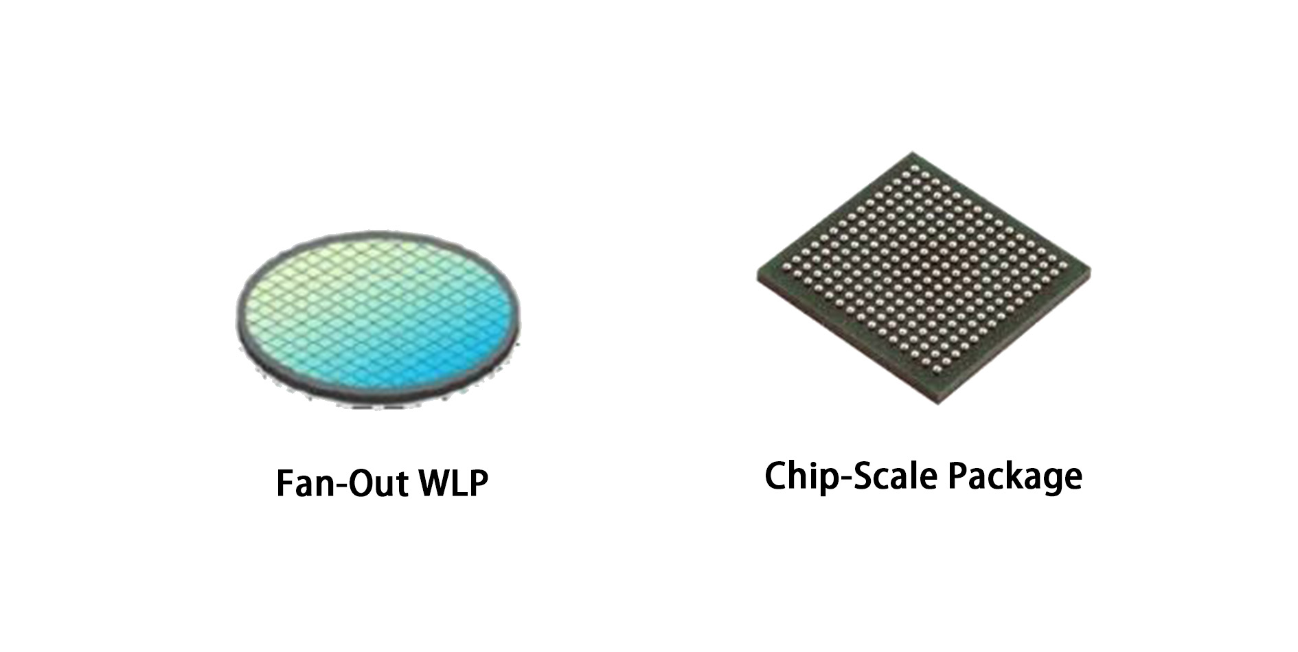
1. Fan-Out Wafer-Level Bundling (Fan-Out WLP):This procedure expands the bundling substrate around the wafer through uncommon forms, making the chip bundling more compact. It is exceedingly appropriate for applications requiring tall integration, altogether moving forward bundling thickness and execution.
2. Chip-Scale Bundling (CSP):Chip-scale bundling may be a profoundly compact bundling innovation whose estimate is nearly the same as the chip itself. Since it regularly does not require holding wires, this bundling shape not as it were significantly diminishes bundling costs but moreover spares space, making it beneficial for applications requiring miniaturization and tall productivity.
Wafer-level bundling speaks to an progressed chip bundling innovation that specifically bundles the chip amid the wafer fabricating prepare. Compared to conventional bundling advances, wafer-level bundling essentially decreases extra bundling steps, upgrades generation productivity, and increments bundling thickness, coming about in a more compact bundle structure.
Related Information

-

-
Phone
+86 135 3401 3447 -
Whatsapp