Cart ( )
Voltage doubler circuit design and application in electronics
2024/3/28 10:06:56
Views:
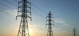
In the field of electronics, it is crucial to improve the circuit design with voltage doubler circuits, which can convert the input voltage into a higher output voltage. The design principle and application range of voltage doubler circuits are very wide, and they are widely used in various electronic equipment and systems, such as power supplies, wireless communication equipment, and medical equipment. By carefully designing the voltage doubler circuit, we can effectively improve system performance and achieve higher efficiency and more stable power output.
Working principle
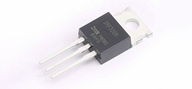
Voltage doubler circuits mainly use the energy storage characteristics of inductors and capacitors to achieve boost conversion from input voltage to output voltage. Typically, a voltage doubler circuit uses an oscillator circuit to generate an alternating current that creates a magnetic field on the inductor. When current flows through the inductor, the magnetic field stores energy. This stored energy is then transferred to the output through appropriate rectification and filtering circuits to obtain a high voltage output.
Specifically, voltage doubling circuits achieve voltage conversion by periodically switching circuit elements, such as diodes, transistors, or power field-effect transistors. This periodic switching operation results in the exchange of energy between the inductor and capacitor, ultimately converting the input voltage into the desired output voltage. This working principle makes the voltage doubler circuit a very efficient voltage boosting solution.
Classification
A boost voltage doubler circuit is the most common type and boosts the input voltage to an output voltage. This circuit design achieves high-efficiency boost conversion through reasonable selection of inductor and capacitor parameters, as well as optimization of switching frequency and duty cycle.
The flyback voltage doubler circuit is a common pulse power conversion circuit. It contains a transformer to achieve voltage conversion and is often used in high power applications. This circuit design is usually simple in structure, but requires careful design to ensure stability and efficiency.
A mutual inductance voltage doubler circuit is a circuit structure that uses a mutual inductor (transformer) to achieve voltage conversion. Through the coupling and transformation ratio of the transformer, the input voltage can be boosted to a high voltage output.
Application
Voltage doubler circuits play an important role in various electronic devices and systems. Here are a few typical application scenarios:
1. Power supply: Modern electronic devices such as mobile phones, tablets, wireless routers, etc. usually require power supplies with multiple different voltage levels. Voltage doubler circuits can be used to adjust the input voltage to meet the device's needs for different voltages.
2. LED driver: LED lighting systems usually require constant current drive, while the input voltage may fluctuate. The voltage doubler circuit can provide stable output voltage and current to ensure the normal operation of the LED.
3. Wireless communication equipment: In wireless communication equipment, it is often necessary to convert low voltage into high voltage to drive radio frequency amplifiers or antennas. Voltage doubler circuits play a key role in these scenarios to ensure the normal operation of the equipment and communication quality.
4. Solar charging system: The solar charging system converts solar energy into electrical energy, but the output voltage may be unstable. Voltage doubler circuits can be used to step up the low voltage produced by solar panels to a level suitable for recharging batteries.
Working principle
Voltage doubler circuits mainly use the energy storage characteristics of inductors and capacitors to achieve boost conversion from input voltage to output voltage. Typically, a voltage doubler circuit uses an oscillator circuit to generate an alternating current that creates a magnetic field on the inductor. When current flows through the inductor, the magnetic field stores energy. This stored energy is then transferred to the output through appropriate rectification and filtering circuits to obtain a high voltage output.
Specifically, voltage doubling circuits achieve voltage conversion by periodically switching circuit elements, such as diodes, transistors, or power field-effect transistors. This periodic switching operation results in the exchange of energy between the inductor and capacitor, ultimately converting the input voltage into the desired output voltage. This working principle makes the voltage doubler circuit a very efficient voltage boosting solution.
Classification
A boost voltage doubler circuit is the most common type and boosts the input voltage to an output voltage. This circuit design achieves high-efficiency boost conversion through reasonable selection of inductor and capacitor parameters, as well as optimization of switching frequency and duty cycle.
The flyback voltage doubler circuit is a common pulse power conversion circuit. It contains a transformer to achieve voltage conversion and is often used in high power applications. This circuit design is usually simple in structure, but requires careful design to ensure stability and efficiency.
A mutual inductance voltage doubler circuit is a circuit structure that uses a mutual inductor (transformer) to achieve voltage conversion. Through the coupling and transformation ratio of the transformer, the input voltage can be boosted to a high voltage output.
Application
Voltage doubler circuits play an important role in various electronic devices and systems. Here are a few typical application scenarios:
1. Power supply: Modern electronic devices such as mobile phones, tablets, wireless routers, etc. usually require power supplies with multiple different voltage levels. Voltage doubler circuits can be used to adjust the input voltage to meet the device's needs for different voltages.
2. LED driver: LED lighting systems usually require constant current drive, while the input voltage may fluctuate. The voltage doubler circuit can provide stable output voltage and current to ensure the normal operation of the LED.
3. Wireless communication equipment: In wireless communication equipment, it is often necessary to convert low voltage into high voltage to drive radio frequency amplifiers or antennas. Voltage doubler circuits play a key role in these scenarios to ensure the normal operation of the equipment and communication quality.
4. Solar charging system: The solar charging system converts solar energy into electrical energy, but the output voltage may be unstable. Voltage doubler circuits can be used to step up the low voltage produced by solar panels to a level suitable for recharging batteries.
Related Information
-

-
Phone
+86 135 3401 3447 -
Whatsapp