Cart ( )
Deeply understand the design principles of pull-down resistors for transistors and MOS tubes
2024/5/27 14:26:21
Views:
1. Transistor, Rce≈0, Vce≈0.3V, 0.3V is directly grounded. Ib≥1mA, if Ib=1mA, Ic=100mA, β=100, the transistor is fully turned on. NPN transistor. Basic knowledge article: Four formulas, play with transistors! Base pull-down resistor: most current-type drive components have a base series current limiting resistor of less than or equal to 10K.
The temperature switch is similar to a key switch in that it regulates the motor's start and stop. B series switch, N tube as switch tube. The motor DC has brushes, the positive 12V is connected, the negative grounded, and the motor rotates. The temperature switch is turned on, CE is fully turned on, Vce » 0.3V, the motor voltage drop is close to 12V, because be conduction impedance is less than 2K resistor R2, most of the current flows to the transistor; the temperature switch is disconnected, ib has no current, and ic has no current. At the moment the temperature switch is turned off, the current of the transistor ib and ic drops to zero all at once, and then slowly drops to zero. This manufacturing process is inevitable. During this time, the transistor working amplification area is most disturbed. Therefore, a pull-down resistor R2 is required. The resistor provides a discharge circuit for the transistor, and point A provides an energy dispersion path. Discharge circuit understanding? Capacitors C1, C2, and C3 for transistors BE, BC, and CE; parasitic capacitance of transistors; real process manufacturing model of transistors. With the existence of capacitors, the transistor is bound to delay. Loop I is formed when capacitor C1 discharges when there is no current in ib. At this point, the amplification region is vulnerable to interference as B's voltage declines from 0.7V to 0V. Resistors R2 are added across C1, and part of the capacitor charge is released by resistor R2. The capacitor discharges more quickly the lower the resistance value. Resistor R2 releases the charge to the capacitor path, shortening the working amplification time of the transistor.
Energy provides a dispersion path understanding? For point A, resistor R2 offers an energy dispersion channel. Point A is suspended, its voltage is erratic, and it is in a high-resistance condition (infinite impedance) when the temperature switch is unplugged. It is easy to mislead and is also affected by the surrounding environment, such as static electricity and lightning damage. The A pull-down resistor is grounded, and most current goes into the ground along the resistor in the event of lightning strikes in the working environment and high-voltage static electricity. This creates a scattered channel for energy. Without a resistor, when lightning strikes, the impedance on the left side of A is infinite, and the right side of A is connected to a transistor, the impedance is relatively low, and all the current flows into the transistor in the direction of low impedance, causing excessive current and permanent damage to the device. MOS tube, to prevent static electricity from causing no charge release circuit, which is easy to cause static electricity breakdown. MOS tube works in the switch state, continuously charging and discharging Cgs. CGS maintains charge internally when the power is off, but there isn't a release circuit. The parameters necessary to create a conductive channel are still there, as is the MOS tube gate electric field. The MOS tube instantly produces an uncontrolled drain current Id the next time the power is turned on due to the conductive channel's activity, which burns the MOS tube out.
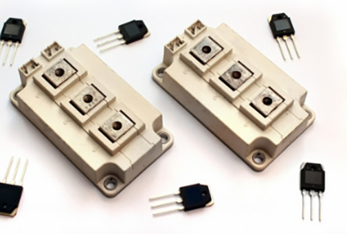
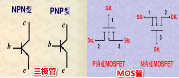
Introduction to transistor MOS tubes Two commonly used semiconductor components, transistor MOS tubes, have only three pins. The transistors are NPN and PNP types, with three electrodes: base B, collector C, emitter E; MOS tube drain D, source S, gate G three electrodes, the middle arrow represents the substrate, the arrow inward is the N-channel MOS tube, and the arrow outward is the P-channel MOS tube.
Triode MOS tube pull-down resistor design
Triode application switching circuit, signal amplification circuit, level conversion circuit, MOS tube amplification circuit, switching circuit, sometimes the two have the same effect, such as small load switching circuit.
2. The role of pull-down resistors for transistors and MOS tubes
Transistor current-type driving components, base series current limiting resistors, generally less than 10K, typical values are 3.3K, 4.7K, 5.1K, 6.8K, etc., but what about the base pull-down resistor?
Design of pull-down resistors for transistor MOS tubes
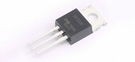
Transistor 8050 switching circuit, the transistor is turned on when the I/O port outputs a high level, and the transistor is not turned on when the input is a low level, but the base B68K pull-down resistor, even if the I/O port does not output a high level, the base is always pulled down and is in the cut-off state. Without resistance, the circuit may be in an unstable state, especially when it is initialized after power-on, it is easy to cause noise, causing the transistor to malfunction, especially for general input/output ports. This resistor is actually a bias resistor, which pulls down the base without a drive signal, making the circuit more reliable.
Adding pull-down makes the circuit more reliable, but the resistor cannot be too large or too small. The base current is insufficient to drive the transistor if it is too large. If it is too small, the bias voltage will be less than the transistor d conduction voltage. Generally, the resistance is not greater than 100K.
Sometimes the resistor is connected in parallel with the capacitor. Generally, the performance of adding capacitor is improved in the design of high-speed signal switching circuit.
3.Third, MOS tubes are different. MOS tubes are voltage-controlled components, voltage-driven, parasitic capacitance between MOS tube pins, and actual capacitance charging and discharging when MOS tubes are turned on. N-type MOS tubes are turned on when Vgs is greater than a certain value, and P-type MOS tubes are turned on when Vgs is less than a certain value.
Due to the capacitance effect between the pins, the parasitic capacitance voltage is properly discharged when the MOS tube is turned off, similar to the discharge resistor, MOS tube protection.
The temperature switch is similar to a key switch in that it regulates the motor's start and stop. B series switch, N tube as switch tube. The motor DC has brushes, the positive 12V is connected, the negative grounded, and the motor rotates. The temperature switch is turned on, CE is fully turned on, Vce » 0.3V, the motor voltage drop is close to 12V, because be conduction impedance is less than 2K resistor R2, most of the current flows to the transistor; the temperature switch is disconnected, ib has no current, and ic has no current. At the moment the temperature switch is turned off, the current of the transistor ib and ic drops to zero all at once, and then slowly drops to zero. This manufacturing process is inevitable. During this time, the transistor working amplification area is most disturbed. Therefore, a pull-down resistor R2 is required. The resistor provides a discharge circuit for the transistor, and point A provides an energy dispersion path. Discharge circuit understanding? Capacitors C1, C2, and C3 for transistors BE, BC, and CE; parasitic capacitance of transistors; real process manufacturing model of transistors. With the existence of capacitors, the transistor is bound to delay. Loop I is formed when capacitor C1 discharges when there is no current in ib. At this point, the amplification region is vulnerable to interference as B's voltage declines from 0.7V to 0V. Resistors R2 are added across C1, and part of the capacitor charge is released by resistor R2. The capacitor discharges more quickly the lower the resistance value. Resistor R2 releases the charge to the capacitor path, shortening the working amplification time of the transistor.
Energy provides a dispersion path understanding? For point A, resistor R2 offers an energy dispersion channel. Point A is suspended, its voltage is erratic, and it is in a high-resistance condition (infinite impedance) when the temperature switch is unplugged. It is easy to mislead and is also affected by the surrounding environment, such as static electricity and lightning damage. The A pull-down resistor is grounded, and most current goes into the ground along the resistor in the event of lightning strikes in the working environment and high-voltage static electricity. This creates a scattered channel for energy. Without a resistor, when lightning strikes, the impedance on the left side of A is infinite, and the right side of A is connected to a transistor, the impedance is relatively low, and all the current flows into the transistor in the direction of low impedance, causing excessive current and permanent damage to the device. MOS tube, to prevent static electricity from causing no charge release circuit, which is easy to cause static electricity breakdown. MOS tube works in the switch state, continuously charging and discharging Cgs. CGS maintains charge internally when the power is off, but there isn't a release circuit. The parameters necessary to create a conductive channel are still there, as is the MOS tube gate electric field. The MOS tube instantly produces an uncontrolled drain current Id the next time the power is turned on due to the conductive channel's activity, which burns the MOS tube out.
Introduction to transistor MOS tubes Two commonly used semiconductor components, transistor MOS tubes, have only three pins. The transistors are NPN and PNP types, with three electrodes: base B, collector C, emitter E; MOS tube drain D, source S, gate G three electrodes, the middle arrow represents the substrate, the arrow inward is the N-channel MOS tube, and the arrow outward is the P-channel MOS tube.
Triode MOS tube pull-down resistor design
Triode application switching circuit, signal amplification circuit, level conversion circuit, MOS tube amplification circuit, switching circuit, sometimes the two have the same effect, such as small load switching circuit.
2. The role of pull-down resistors for transistors and MOS tubes
Transistor current-type driving components, base series current limiting resistors, generally less than 10K, typical values are 3.3K, 4.7K, 5.1K, 6.8K, etc., but what about the base pull-down resistor?
Design of pull-down resistors for transistor MOS tubes
Transistor 8050 switching circuit, the transistor is turned on when the I/O port outputs a high level, and the transistor is not turned on when the input is a low level, but the base B68K pull-down resistor, even if the I/O port does not output a high level, the base is always pulled down and is in the cut-off state. Without resistance, the circuit may be in an unstable state, especially when it is initialized after power-on, it is easy to cause noise, causing the transistor to malfunction, especially for general input/output ports. This resistor is actually a bias resistor, which pulls down the base without a drive signal, making the circuit more reliable.
Adding pull-down makes the circuit more reliable, but the resistor cannot be too large or too small. The base current is insufficient to drive the transistor if it is too large. If it is too small, the bias voltage will be less than the transistor d conduction voltage. Generally, the resistance is not greater than 100K.
Sometimes the resistor is connected in parallel with the capacitor. Generally, the performance of adding capacitor is improved in the design of high-speed signal switching circuit.
3.Third, MOS tubes are different. MOS tubes are voltage-controlled components, voltage-driven, parasitic capacitance between MOS tube pins, and actual capacitance charging and discharging when MOS tubes are turned on. N-type MOS tubes are turned on when Vgs is greater than a certain value, and P-type MOS tubes are turned on when Vgs is less than a certain value.
Due to the capacitance effect between the pins, the parasitic capacitance voltage is properly discharged when the MOS tube is turned off, similar to the discharge resistor, MOS tube protection.
Related Information

-

-
Phone
+86 135 3401 3447 -
Whatsapp