Cart ( )
Exploring the Impact of Transient Loads on Power Systems: Low Frequency Sine Wave Generation
2024/6/3 11:06:31
Views:
The term "load transient" describes a momentary shift in load current. This sudden change is called a load transient. The load transient responsiveness of a voltage regulator is its capacity to maintain a steady output voltage during a load transient. When the load current varies gradually, it is easy to maintain a constant output voltage; but, when the load current varies quickly, the output voltage will likewise fluctuate. Load transient performance is defined by how much the output voltage changes.
The key principles are as follows:
1) Think of the voltage regulator as a voltage-controlled current source, with the current from the load driving the regulator (a voltage-regulated current source fed back from the output). The regulator's current source does not change during zero time, so if the load current changes quickly enough, the output voltage will change accordingly. The pace at which the load current fluctuates, the quantity and kind of output capacitors, and the regulator's speed all affect how much of a change there is.
2) During the time it takes the regulator's control loop to adjust to the load change, the only thing that provides the difference between the previous steady-state load current value and the new value is the output capacitors. Therefore, the key to controlling the output voltage during a load transient lies in the output capacitors, and the electrical characteristics of these capacitors can significantly affect the transient response.
3) The output capacitor voltage varies less before the regulator control loop adjusts to the new load current value the faster the loop responds. It follows that in order to maintain the same VOUT tolerance range, a faster regulator might use smaller output capacitors, which can save costs.
A power system's transient response can be tested with fast dynamic loads, which can reveal a number of important operational features. A quick current step can create a voltage divergence that can reveal information about the phase margin of the regulator. Furthermore, transient testing can assist in determining the effective series connection inductance, shunt capacitance, and ESR for power supplies that are situated at a distance from the load point. While the provider frequently verifies the phase margin on commercial power supplies, adding remote sensing frequently causes the power supply to become unstable. Interconnect inductance and load capacitance can introduce additional phase shifts in the regulator control loop feedback, affecting stability.
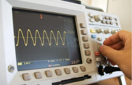
Engineers have seen low-frequency sine waves on the regulator output. Performing transient testing can quickly check the dynamic regulation stability and accuracy of the system. Since most commercial dynamic electronic loads have very sluggish current slew rates, testing quicker regulator control loops-which can usually reach steady state in 50µs or less after a significant load transient-may find it more difficult to employ these loads. Many high power systems require current slew rates of 10A/µs or more.
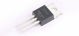
This is an adaptation of the application note with some notable improvements. Maximum power has been increased to 150W, and is designed for 3.3V, 5V, and 12V regulator outputs. One N-channel low-side MOSFET switches a resistive load made up of R1–R3. Numerous different load combinations are made feasible by the size and population of the load resistors.
A relaxation oscillator with Q2, R8, R9, and C3 is built using Schmitt trigger inputs by MOSFET driver U1, the main part of the circuit.The duty cycle and cycle time for the component values displayed are roughly 5% and 20 ms, respectively. Significantly lower duty cycle allows for a moderate cooling solution.
R6 and R7, taken separately, change the rise and fall timings in conjunction with the MOSFET's CISS input capacitance. With the values shown, the rise and fall times are approximately 1µs. The highest MOSFET gate current at this slew rate is roughly +110/-75 mA, which is significantly less than U1's 1.4A maximum current limit. To further reduce the edge rate, add C2. The MOSFET gate switching resonance is not significant due to the 1µs rise/fall times and the added dissipative damping of the relatively large gate resistor. In order to reduce line resonance when the MOSFET is turned off, R4 and C1 are used. The input capacitance and effective line inductance influence R4's value. It has been found that 0.5O works well for most wiring situations.
The two-wire connection to the DUT is one of this implementation's more practical features. A 12V boost converter is supplied to power the MOSFET driver and gate in 3.3V and 5V systems. Additional power supply or connections are not needed. The maximum current that can be supplied to charge the MOSFET gate may be limited by the boost converter's output, which can supply roughly 350mA from a 3.3V input. For quicker current edge speeds, an initial gate charging current is provided by the low ESR aluminum capacitor C5. A direct connect version that operates at 12V can be made by swapping out C7 for a 0O resistor, which will turn off the boost converter. Although there will be some voltage loss across L1 and D2, the circuit will still function normally despite this.
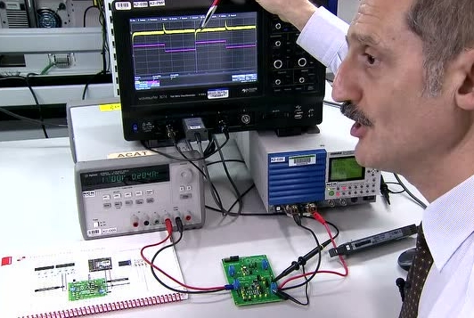
A 3" × 5" two-layer PCB can accommodate the complete circuit, including the heat sink and a tiny 12V fan, without becoming uncomfortable. Basic operation only requires the connection of two wires.
To stop the lead reactance from ringing, the tester leads need to be short and low inductance. DUT connections ought to be placed close to a remote sense site or the point of load. The return leads of the voltage probe and the tester common should be linked in one place. Selecting a location with a low impedance connection back to the power source is also crucial.
When the momentary pushbutton PB1 is pressed, the astable circuit is initiated, causing the dynamic load to switch. If needed, a static PSU load can be supplied externally. A practical high bandwidth method for sensing pulsed current is offered by R5 and J2. To monitor 1mV/A of current, a straight 50Ω coaxial cable can be connected directly to the oscilloscope input. Additionally, voltage measurements must be AC linked to a second oscilloscope input and taken close to the point of load or a remote sensing point. When probing voltage, caution must be used. Measurements that are inaccurate can be caused by probe inductance from far-off ground or return lines. To further reduce high frequency ringing from the probe ESL, a tiny series resistor (a few ohms) can be placed to the probe tip.
The key principles are as follows:
1) Think of the voltage regulator as a voltage-controlled current source, with the current from the load driving the regulator (a voltage-regulated current source fed back from the output). The regulator's current source does not change during zero time, so if the load current changes quickly enough, the output voltage will change accordingly. The pace at which the load current fluctuates, the quantity and kind of output capacitors, and the regulator's speed all affect how much of a change there is.
2) During the time it takes the regulator's control loop to adjust to the load change, the only thing that provides the difference between the previous steady-state load current value and the new value is the output capacitors. Therefore, the key to controlling the output voltage during a load transient lies in the output capacitors, and the electrical characteristics of these capacitors can significantly affect the transient response.
3) The output capacitor voltage varies less before the regulator control loop adjusts to the new load current value the faster the loop responds. It follows that in order to maintain the same VOUT tolerance range, a faster regulator might use smaller output capacitors, which can save costs.
A power system's transient response can be tested with fast dynamic loads, which can reveal a number of important operational features. A quick current step can create a voltage divergence that can reveal information about the phase margin of the regulator. Furthermore, transient testing can assist in determining the effective series connection inductance, shunt capacitance, and ESR for power supplies that are situated at a distance from the load point. While the provider frequently verifies the phase margin on commercial power supplies, adding remote sensing frequently causes the power supply to become unstable. Interconnect inductance and load capacitance can introduce additional phase shifts in the regulator control loop feedback, affecting stability.
Engineers have seen low-frequency sine waves on the regulator output. Performing transient testing can quickly check the dynamic regulation stability and accuracy of the system. Since most commercial dynamic electronic loads have very sluggish current slew rates, testing quicker regulator control loops-which can usually reach steady state in 50µs or less after a significant load transient-may find it more difficult to employ these loads. Many high power systems require current slew rates of 10A/µs or more.
This is an adaptation of the application note with some notable improvements. Maximum power has been increased to 150W, and is designed for 3.3V, 5V, and 12V regulator outputs. One N-channel low-side MOSFET switches a resistive load made up of R1–R3. Numerous different load combinations are made feasible by the size and population of the load resistors.
A relaxation oscillator with Q2, R8, R9, and C3 is built using Schmitt trigger inputs by MOSFET driver U1, the main part of the circuit.The duty cycle and cycle time for the component values displayed are roughly 5% and 20 ms, respectively. Significantly lower duty cycle allows for a moderate cooling solution.
R6 and R7, taken separately, change the rise and fall timings in conjunction with the MOSFET's CISS input capacitance. With the values shown, the rise and fall times are approximately 1µs. The highest MOSFET gate current at this slew rate is roughly +110/-75 mA, which is significantly less than U1's 1.4A maximum current limit. To further reduce the edge rate, add C2. The MOSFET gate switching resonance is not significant due to the 1µs rise/fall times and the added dissipative damping of the relatively large gate resistor. In order to reduce line resonance when the MOSFET is turned off, R4 and C1 are used. The input capacitance and effective line inductance influence R4's value. It has been found that 0.5O works well for most wiring situations.
The two-wire connection to the DUT is one of this implementation's more practical features. A 12V boost converter is supplied to power the MOSFET driver and gate in 3.3V and 5V systems. Additional power supply or connections are not needed. The maximum current that can be supplied to charge the MOSFET gate may be limited by the boost converter's output, which can supply roughly 350mA from a 3.3V input. For quicker current edge speeds, an initial gate charging current is provided by the low ESR aluminum capacitor C5. A direct connect version that operates at 12V can be made by swapping out C7 for a 0O resistor, which will turn off the boost converter. Although there will be some voltage loss across L1 and D2, the circuit will still function normally despite this.
A 3" × 5" two-layer PCB can accommodate the complete circuit, including the heat sink and a tiny 12V fan, without becoming uncomfortable. Basic operation only requires the connection of two wires.
To stop the lead reactance from ringing, the tester leads need to be short and low inductance. DUT connections ought to be placed close to a remote sense site or the point of load. The return leads of the voltage probe and the tester common should be linked in one place. Selecting a location with a low impedance connection back to the power source is also crucial.
When the momentary pushbutton PB1 is pressed, the astable circuit is initiated, causing the dynamic load to switch. If needed, a static PSU load can be supplied externally. A practical high bandwidth method for sensing pulsed current is offered by R5 and J2. To monitor 1mV/A of current, a straight 50Ω coaxial cable can be connected directly to the oscilloscope input. Additionally, voltage measurements must be AC linked to a second oscilloscope input and taken close to the point of load or a remote sensing point. When probing voltage, caution must be used. Measurements that are inaccurate can be caused by probe inductance from far-off ground or return lines. To further reduce high frequency ringing from the probe ESL, a tiny series resistor (a few ohms) can be placed to the probe tip.
Related Information
-

-
Phone
+86 135 3401 3447 -
Whatsapp