Cart ( )
Core Protection in Modern Semiconductor Packaging
2024/7/19 15:45:27
Views:
With the fast improvement of cutting edge innovation, semiconductor bundling, as one of the key innovations, is playing an irreplaceable part. It typifies the modest and delicate semiconductor chips in a defensive shell, ensuring the chips and encouraging their association to circuit sheets. This article will detail the definition, standards, and different application sorts of semiconductor bundling.
1. Definition and Standards of Semiconductor Bundling
Semiconductor bundling alludes to the method of typifying semiconductor chips in microelectronic gadgets with defensive shells. Regularly, bundling includes interfacing the chip to a bundle base or substrate and covering it with bundling materials (such as plastic, ceramic, or metal). The most reason of bundling is to secure the semiconductor chip from mechanical, chemical, or natural harm and to supply electrical associations for the chip.
The most standards of semiconductor bundling incorporate the taking after perspectives:
1. Ensuring the chip: Semiconductor chips are exceptionally little and delicate, helpless to outside natural impacts. Bundling gives a defensive layer to anticipate the chip from physical harm, clean, dampness, and erosion.
2. Electrical association: Bundling interfaces the chip to outside circuit sheets through pins or cushions, empowering communication and operation with other components.
3. Warm scattering and electromagnetic protecting: The bundling plan as a rule incorporates warm sinks and protecting layers to successfully scatter warm and square electromagnetic impedances, guaranteeing the steady operation of the chip.
2. Sorts of Semiconductor Bundling Applications
Semiconductor bundling encompasses a wide extend of applications in different areas, and here are a few major application sorts:
1. Inserted frameworks: Semiconductor bundling is broadly utilized in implanted frameworks such as smartphones, tablets, and IoT gadgets, ensuring the chip and giving electrical associations.
2. Electronic customer items: In electronic gadgets like TVs, sound frameworks, and cameras, chip bundling permits association with other components and gives assurance.
3. Car industry: The expanding number of electronic components in cars requires exceedingly dependable semiconductor bundling innovation to adjust to cruel natural conditions.
4. Therapeutic gear: Semiconductor bundling plays an critical part in therapeutic gadgets such as pacemakers, observing gadgets, and restorative imaging hardware.
5. Mechanical control and robotization: In mechanical gadgets like PLCs (Programmable Rationale Controllers), sensors, and drivers, bundling secures the chip, guaranteeing steady operation in unforgiving mechanical situations.
6. Communication and organize hardware: Semiconductor chips in communication and organize gear ought to adjust to high-frequency and high-speed transmission necessities, and bundling gives segregation and protection in these gadgets.
3. Various Forms of Semiconductor Packaging
Semiconductor packaging comes in many forms to meet different application needs:
1. Die-Level Bundling: This includes bundling person chips, more often than not utilizing no-lead (Flip Chip) or few-lead (BGA, CSP) shapes, fundamentally utilized in high-density coordinates circuits and miniaturized scale sensors.
2. Inactive Component Bundling: This includes bundling inactive components like resistors, capacitors, and inductors to supply mechanical security and easy-to-solder stick interfacing.
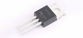
3. Little Flag and Control Semiconductor Bundling: This includes bundling little flag and control semiconductor gadgets like diodes, transistors, and control modules. Common shapes incorporate TO-92, TO-220, SOT-23, and Plunge.
4. Microelectronics Bundling: This includes bundling microelectronic gadgets like MEMS (Micro-Electro-Mechanical Systems) and optoelectronic components to supply assurance and association.
5. High-Reliability Bundling: Utilized in military, aviation, and car areas, this bundling requires exceedingly solid shapes.
Conclusion
In conclusion, semiconductor packaging meets different application needs by adopting various forms and materials, providing chip protection, connection, and adaptation functions. The persistent advance in semiconductor bundling innovation will advance advancement and advancement within the semiconductor application field, advance progressing cutting edge innovation. Whether in inserted frameworks, electronic shopper items, the car industry, restorative hardware, mechanical control, or communication hardware, semiconductor bundling plays a vital part. Within the future, with continuous innovative headways, bundling innovation will see more advancements and breakthroughs.
Related Information

-

-
Phone
+86 135 3401 3447 -
Whatsapp