Cart ( )
Optimize the power supply PCB layout scheme to reduce the electromagnetic interference level
2024/5/31 14:16:27
Views:
In EMC product design, the importance of PCB design cannot be ignored, in addition to selecting appropriate components and circuit design. The key is to minimize the return flow area of the signal and ensure that the return flow path flows in the intended direction. Layer design is the basis of PCB. Reasonable PCB layer design can greatly optimize EMC performance.
One of the core strategies is to precisely plan the PCB stackup structure to optimize the signal return path, with the goal of minimizing or eliminating magnetic flux. Among them, the mirror layer-the copper plane layer (power layer or ground layer) next to the signal layer-plays a key role: reducing return noise, especially in power distribution systems with large current flow, significantly reducing EMI, and controlling high-speed digital circuits. Crosstalk, and control crosstalk interference by adjusting the distance between the signal line and the mirror layer, and achieve impedance control to prevent signal reflection.
When discussing the EMC design challenges of switching power supplies, the precise implementation of PCB layout is one of the challenges. The design process requires consideration of many factors, such as electrical performance, manufacturing processes, safety regulations, and EMC effects. EMC is the most difficult factor to grasp and often becomes a bottleneck for project progress. Next, I will share the relationship between PCB layout and EMC from several directions.
For example, the design of sampled signals requires special attention. Pull the signal from the sampling resistor, making sure the IC's ground is referenced to the sampling resistor. In addition, the driving signals should be routed to avoid interfering with critical CS signals. In the wiring design, placing the ground wire between the drive line and CS line can play a shielding role.
The ground connection of the main power and control parts is also crucial. Making sure that every component is attached to its respective position accurately is essential. For example, the PFC driver and IC should be grounded together. The driving ground and control ground of the DC-DC part are grounded to the sampling ground of the DC switching tube part.
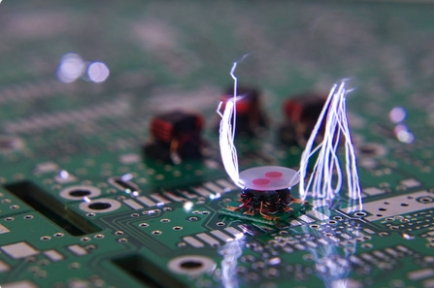
Electromagnetic field shielding analysis, input and output electric field interference are usually transmitted through capacitive coupling. Adding shielding plates can change this dynamic and effectively reduce interference. Magnetic field shielding requires more complex housing shielding.
For switching devices, their EMC performance is significantly affected by their switching speed. Although the use of fast switching devices can improve efficiency, in order to meet EMC requirements, efficiency may need to be sacrificed to reduce switching speed, thereby weakening radiated interference.
Filter design is equally critical. Choosing the appropriate filter architecture and materials can significantly improve filtering results. The design of the filter should be optimized according to the impedance matching principle to achieve the best filtering performance.
In summary, PCB design plays a central role in controlling EMC. Reducing backflow noise and EMI, and controlling crosstalk and impedance through reasonable layer design and signal path planning are key strategies to optimize EMC performance.
Related Information


-

-
Phone
+86 135 3401 3447 -
Whatsapp