Cart ( )
Full analysis of PCB packaging types: choose the most suitable packaging method
2024/3/6 9:55:33
Views:
PCB (printed circuit board) packaging is the process of connecting an integrated circuit chip (IC) to a PCB and communicating with other electronic components through external pins. In modern electronic equipment, PCB packaging plays a vital role, not only protecting the chip from environmental influences, but also enabling the expansion and interconnection of circuit functions.
Definition and types of PCB packaging
1. Definition of PCB packaging
PCB packaging is the encapsulation of an exposed integrated circuit chip (IC) in a specific housing or packaging material so that it can be mounted on a printed circuit board (PCB) and connected to other components. Encapsulation not only provides physical protection, but also provides electrical connections and thermal management functions. The design and selection of PCB packaging have an important impact on circuit performance, stability and reliability.
2. Types of PCB packaging
PCB packaging is mainly divided into the following types:
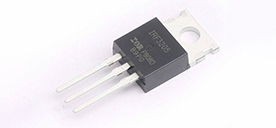
- DIP packaging, or dual in-line packaging, is a traditional integrated circuit packaging form, usually used in earlier integrated circuits. It has two rows of pins and can be plugged directly into a printed circuit board (PCB), making it suitable for some applications that require high stability and reliability.
- SMD package: Surface Mount Device, surface mount package, suitable for modern high-density PCB design, can be directly fixed on the PCB surface through welding, saving space and improving production efficiency.
- BGA package, also known as Ball Grid Array package, uses spherical solder beads to connect, has better heat dissipation performance and circuit transmission performance, and is widely used in high-performance processors and storage devices.
- QFN package: Quad Flat No-leads. With its small size and excellent heat dissipation, it is suitable for scenarios that require compactness, such as mobile devices and radio frequency applications.
PCB packaging manufacturing process
The manufacturing process of PCB packaging includes the following steps:
1. Design packaging drawings: Design the packaging structure and pin layout based on chip size and pin spacing.
2. Make molds: According to the packaging design requirements, make plastic or metal molds for injection molding of packaging materials to form packaging shells.
3. Welding pins: The chip pins are welded to the bottom of the package through automated equipment to form electrical connections.
4. Filling medium: Filling encapsulation material, such as epoxy resin or silicone, to protect and fix the chip.
5. Testing and verification: Conduct chip testing and verification after packaging to ensure that the packaging is intact and meets electrical specifications.
Application areas of PCB packaging
PCB packaging is widely used in the electronics industry, involving the following fields:
- Consumer electronics: mobile phones, tablets, smart home products, etc., require packages of various sizes and performance to achieve different functions.
- Industrial control: Sensors, drivers, etc. in industrial control equipment and automation systems require high temperature resistance and anti-interference packaging.
- Automotive electronics: ECUs, sensors, control modules, etc. in automotive electronic systems require high-temperature and vibration-resistant packaging to cope with harsh environments.
- Aerospace: PCB packages used in aerospace equipment such as aircraft and satellites need to be lightweight, highly reliable and radiation resistant.
- Energy industry: Smart meters, solar inverters, battery management systems and other fields require packaging with efficient heat dissipation and low power consumption.
Definition and types of PCB packaging
1. Definition of PCB packaging
PCB packaging is the encapsulation of an exposed integrated circuit chip (IC) in a specific housing or packaging material so that it can be mounted on a printed circuit board (PCB) and connected to other components. Encapsulation not only provides physical protection, but also provides electrical connections and thermal management functions. The design and selection of PCB packaging have an important impact on circuit performance, stability and reliability.
2. Types of PCB packaging
PCB packaging is mainly divided into the following types:
- DIP packaging, or dual in-line packaging, is a traditional integrated circuit packaging form, usually used in earlier integrated circuits. It has two rows of pins and can be plugged directly into a printed circuit board (PCB), making it suitable for some applications that require high stability and reliability.
- SMD package: Surface Mount Device, surface mount package, suitable for modern high-density PCB design, can be directly fixed on the PCB surface through welding, saving space and improving production efficiency.
- BGA package, also known as Ball Grid Array package, uses spherical solder beads to connect, has better heat dissipation performance and circuit transmission performance, and is widely used in high-performance processors and storage devices.
- QFN package: Quad Flat No-leads. With its small size and excellent heat dissipation, it is suitable for scenarios that require compactness, such as mobile devices and radio frequency applications.
PCB packaging manufacturing process
The manufacturing process of PCB packaging includes the following steps:
1. Design packaging drawings: Design the packaging structure and pin layout based on chip size and pin spacing.
2. Make molds: According to the packaging design requirements, make plastic or metal molds for injection molding of packaging materials to form packaging shells.
3. Welding pins: The chip pins are welded to the bottom of the package through automated equipment to form electrical connections.
4. Filling medium: Filling encapsulation material, such as epoxy resin or silicone, to protect and fix the chip.
5. Testing and verification: Conduct chip testing and verification after packaging to ensure that the packaging is intact and meets electrical specifications.
Application areas of PCB packaging
PCB packaging is widely used in the electronics industry, involving the following fields:
- Consumer electronics: mobile phones, tablets, smart home products, etc., require packages of various sizes and performance to achieve different functions.
- Industrial control: Sensors, drivers, etc. in industrial control equipment and automation systems require high temperature resistance and anti-interference packaging.
- Automotive electronics: ECUs, sensors, control modules, etc. in automotive electronic systems require high-temperature and vibration-resistant packaging to cope with harsh environments.
- Aerospace: PCB packages used in aerospace equipment such as aircraft and satellites need to be lightweight, highly reliable and radiation resistant.
- Energy industry: Smart meters, solar inverters, battery management systems and other fields require packaging with efficient heat dissipation and low power consumption.
Related Information

-

-
Phone
+86 135 3401 3447 -
Whatsapp