Cart ( )
In-depth analysis: Miller effect and countermeasures when MOS tube switches
2024/5/30 11:08:12
Views:
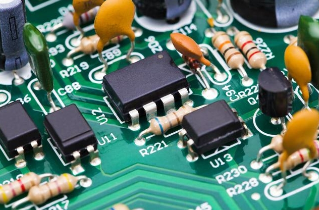
MOSFETs play an important role in modern electronic design, especially in switching circuits. However, when using these components, designers often face the challenge of the Miller effect, which is particularly evident during the gate drive process of the MOSFET. This article will explore the basic principles, effects, and effective solutions of the Miller effect to help designers optimize their circuit designs.
Fundamental ideas
The gate-source capacitance Cgs must be charged and discharged in order for MOSFETs to function. In normal switching operation, when the gate voltage Vgs reaches the threshold voltage, the MOSFET begins to conduct, and then the gate voltage continues to rise, and the device enters the saturation region. However, during this process, due to the existence of the gate-drain capacitance Cgd, that is, the Miller capacitance, a special phenomenon is observed - the Miller platform. At this time, although the input power continues to supply power to the gate, the rise of Vgs is suspended until the drain voltage Vds drops low enough to allow the gate-drain capacitance to be fully charged.
Impact of the Miller Effect
The main impact of the Miller effect is to extend the turn-on time of the MOSFET and increase the energy consumption during the turn-on process. In addition, this effect also affects the switching speed of the device, especially in high-frequency switching applications, where the slowdown may lead to inefficiency and excessive heat. Specifically, the drop in drain voltage Vds is temporarily blocked before Vgs rises high enough to overcome the Miller platform. During this process, the power supply needs to maintain high current output for a longer period of time, increasing the overall loss of the system.
Solutions
There are various strategies to solve the Miller effect, mainly including hardware design improvements and the application of circuit technology. Some common methods include:
1. Use MOSFETs with smaller Cgd: Selecting MOSFETs with smaller gate-drain capacitance can directly reduce the impact of the Miller effect, thereby increasing switching speed and reducing energy loss.
2. Increase drive current: By using a high-current driver to drive the MOSFET, the gate capacitance can be charged and discharged faster, thereby reducing the delay caused by the Miller platform.
3. Optimize circuit design: Adding appropriate bypass capacitors between the gate and source or using specialized drive circuit designs, such as totem pole drive, can effectively mitigate the Miller effect.
4. Software control and adjustment: In some advanced applications, the problems caused by the Miller effect can be indirectly controlled and optimized by controlling the speed and timing of the switch through software.
Practical application
It is particularly important to consider the Miller effect when designing high-efficiency power management systems. For example, in power converters, motor drives, and other applications that require frequent switching, optimizing the selection and driving strategy of MOSFETs can significantly improve the overall performance and efficiency of the system. Through experiments and simulations, designers can better understand the actual impact of the Miller effect under different conditions and optimize the circuit design accordingly.
Conclusion
Although the Miller effect is a challenge in MOSFET design, by understanding its principles, analyzing its impact, and taking effective coping strategies, engineers can overcome this problem, optimize circuit performance, and improve system efficiency. Selecting the right MOSFET, optimizing the drive circuit, designing a reasonable circuit structure, and combining software control and adjustment methods can effectively mitigate the impact of the Miller effect, thereby improving the stability and performance of the circuit. In practical applications, continuous exploration and innovation, combining theory with practice, will provide more possibilities for solving this problem and promote the development of electronic technology.
Related Information

-

-
Phone
+86 135 3401 3447 -
Whatsapp