Cart ( )
SPI Interface Between FPGA and DS1302: An Analysis
2024/7/23 9:35:58
Views:
This article is based on the DS1302 chip and gives a point by point presentation to the SPI communication rule between the chip and FPGA. It clarifies the equipment plan standards and the plan of the FPGA SPI interface driver.
Diagram of the DS1302 Chip
The DS1302, presented by Dallas Semiconductor (presently portion of Adage Coordinates), could be a low-power real-time clock chip that gives data such as seconds, minutes, hours, days, months, and a long time, and incorporates a trickle-charge capability. It is reasonable for applications requiring exact real-time clock capacities. The DS1302 communicates with microprocessors via a simple serial SPI interface, characterized by its simple structure, low power consumption, and high accuracy.
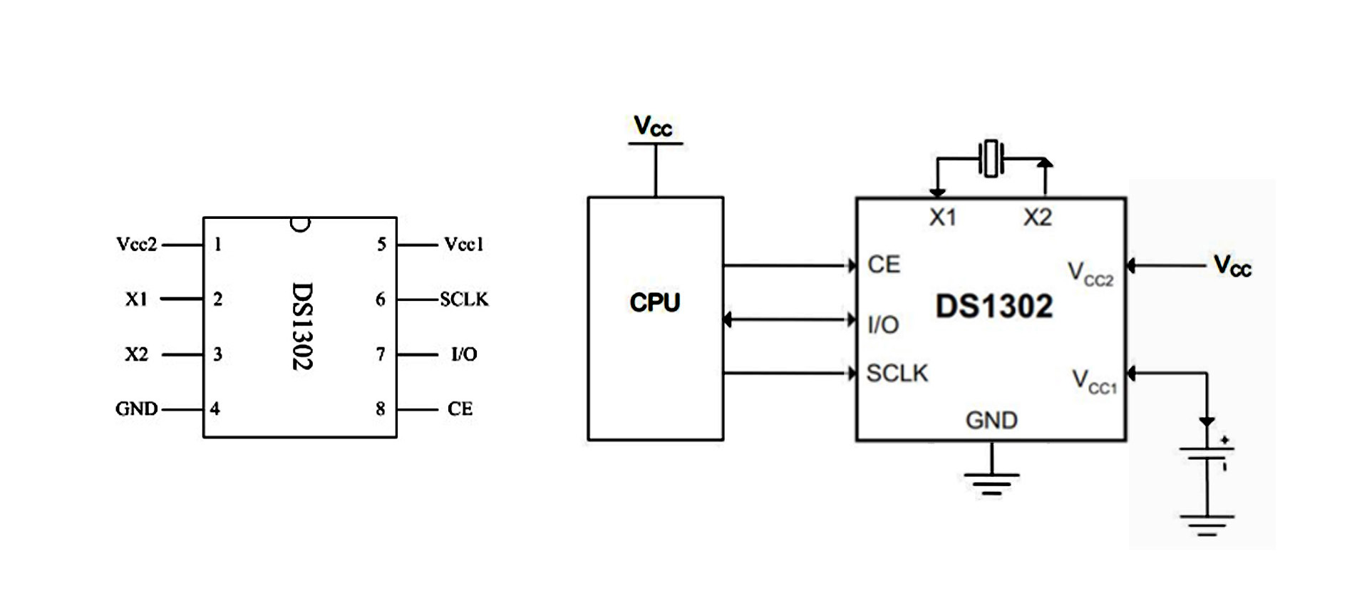
DS1302
SPI Communication Principle between FPGA and DS1302
The SPI interface could be a four-wire communication interface, counting the Serial Clock (SCK), Ace Input/Slave Yield (MISO), Ace Output/Slave Input (MOSI), and a low-level dynamic Slave Select (NSS). The DS1302, as a slave gadget, communicates with the FPGA through the SPI interface. Amid communication, the FPGA acts as the ace gadget, controlling the information transmission timing through the SCK line, sending information to the DS1302 through the MOSI line, and accepting information from the DS1302 by means of the MISO line. The NSS line is utilized to choose the slave gadget, guaranteeing that the ace gadget can communicate with a particular slave gadget.
Hardware Design Principles
In terms of equipment plan, the primary step is to decide the association strategy between the DS1302 and the FPGA. Concurring to the SPI interface definition, the SCK, MISO, MOSI, and GND pins of the DS1302 were given to be associated with the evaluating pins of the FPGA. Besides, to make sure the DS1302 works appropriately, its manipulate pins (VCC1 and VCC2) and clock pins (X1 and X2) want to be related. Pay attention to the following when making connections:
1. Ensure the correctness and stability of the connection lines;
2. Choose appropriate power and clock sources;
3. Pay attention to the layout rationality and electromagnetic compatibility in PCB design.
FPGA SPI Interface Driver Design
When designing the SPI interface driver in the FPGA, the following functions need to be implemented:
1. Generate the SCK signal to control data transmission timing;
2. Send data to the DS1302 via the MOSI line;
3. Receive data from the DS1302 via the MISO line;
4. Control the NSS signal as needed to select the slave device.
During the design process, a state machine approach can be used to design the SPI interface driver. The state machine includes states such as idle, send, and receive. State transitions and data processing are performed based on the current state and input signals. Pay attention to the following points:
1. Ensure the stability and accuracy of the SCK signal;
2. Correctly handle data transmission of the MOSI and MISO signals;
3. Appropriately set the state of the NSS signal as needed to select the slave device.
Conclusion
This article presented the SPI communication guideline between the FPGA and the DS1302 chip, the equipment plan standards, and the plan strategy of the FPGA SPI interface driver. Through this presentation, perusers can get it the essential concepts and characteristics of the SPI interface, ace the fundamental standards and execution strategies of communication between the FPGA and peripherals, and give reference and direction for consequent FPGA plan.
Related Information

-

-
Phone
+86 135 3401 3447 -
Whatsapp