Cart ( )
Ga2O3 Semiconductor: Unlocking the Ga2O3 Bandgap Myster
2023/3/7 9:48:09
Views:
Gallium oxide (Ga2O3) is rising as a groundbreaking fabric within the semiconductor scene. With its special properties and potential applications, Ga2O3 is opening modern roads in electronics and photonics. This article investigates the interesting bandgap of Ga2O3, its comparison with other semiconductors, and its future in different applications.
Future of Semiconductors: Silicon Carbide & Gallium Nitride as Next-Gen Semiconductors
Table of Contents
- What is Ga2O3?
- The Bandgap of Ga2O3
- Advantages of Ga2O3 as a Semiconductor
- Challenges in Ga2O3 Development
- Applications of Ga2O3
- Market Outlook
- The Future of Ga2O3
- Conclusion
- Commonly Asked Questions
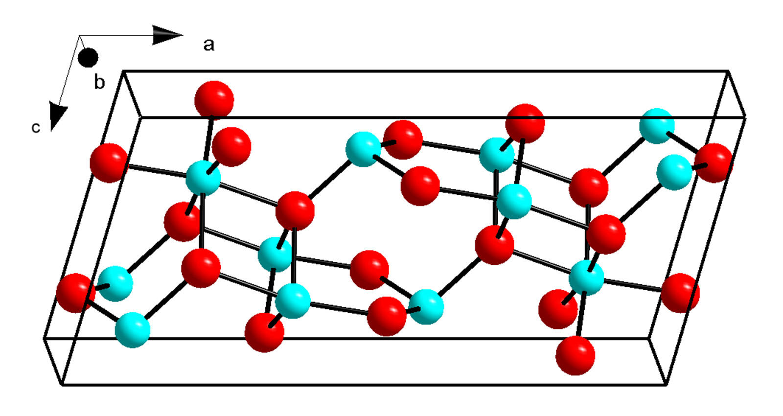
What is Ga2O3?
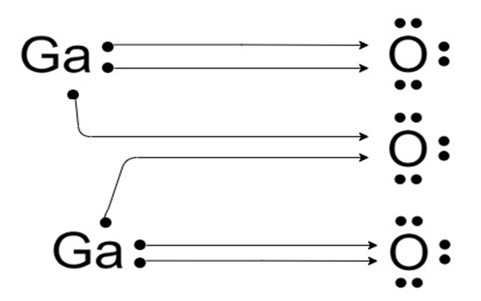
Gallium oxide may well be a twofold compound comprising of gallium and oxygen, frequently showing up in a direct, crystalline shape. It features a put to the family of gallium oxide semiconductors and is picking up thought for its electrical, warm, and optical properties.
Ga2O3 crystal structure
Why is Bandgap Important?
The bandgap of a semiconductor could be a basic parameter that decides its electrical conductivity and potential applications. It is the vitality distinction between the valence band and the conduction band. A more extensive bandgap for the most part permits for operation at higher temperatures and voltages, making it appropriate for high-power applications.
The Bandgap of Ga2O3
Ga₂O₃ has an ultra-wide bandgap of roughly 4.8 eV, situating it among the most noteworthy bandgap materials accessible. This empowers proficient operation in high-temperature and high-voltage situations, making it fundamental for control gadgets.
Comparison of Bandgaps
For comparison, Gan bandgap of about 3.4 eV, while Sic bandgap of around 3.3 eV. The following table summarizes the key characteristics of Ga₂O₃ alongside these semiconductors:
Advantages of Ga2O3 as a Semiconductor
Ultra Wide Band Gap
Ga2O3 is classified as an ultra-wide bandgap semiconductor. This classification suggests that it can productively handle high-energy forms, making it reasonable for different applications in power electronics and optoelectronics. The ultra-wide bandgap allows for low leakage currents, which enhances the efficiency of devices made from Ga2O3.
High Breakdown Voltage
One of the standout features of Ga2O3 is its high breakdown voltage. This property is fundamental for power gadgets, empowering them to function beneath extraordinary conditions without disappointment. Gadgets based on Ga2O3 can handle tall voltages and streams, making them perfect for applications such as control inverters and converters.
Thermal Stability
Ga2O3 shows fabulous thermal stability, permitting gadgets to function productively in high-temperature situations. This property makes Ga2O3 an alluring alternative for applications in car, aviation, and mechanical segments where warm administration is significant.
Challenges in Ga2O3 Development
P-Type Ga2O3
While Ga2O3 has numerous advantages, one of the challenges is achieving p-type Ga2O3. Most current research focuses on n-type Ga2O3, leading to a lack of p-type doping techniques. The ability to produce p-type Ga2O3 is essential for developing efficient bipolar devices and other applications requiring p-n junctions.
Material Quality and Defect Management
Another challenge is the quality of Ga2O3 material. Absconds within the precious stone structure can essentially influence the electrical properties of Ga2O3 semiconductors. Analysts are effectively investigating strategies to make strides the development and manufacture forms to improve fabric quality.
Applications of Ga2O3
Wide Band Gap Semiconductor Applications
Ga2O3 is poised to revolutionize various applications due to its unique properties:
Market Outlook
The worldwide request for high-performance semiconductors is on the rise, driven by the developing selection of electric vehicles, renewable vitality, and progressed electronic frameworks. Ga₂O₃, with its special characteristics, is well-positioned to capture a noteworthy share of this showcase. Here's a market projection showing the rapid growth of the Ga₂O₃ semiconductor market over the coming years:
Ga₂O₃ Market Growth
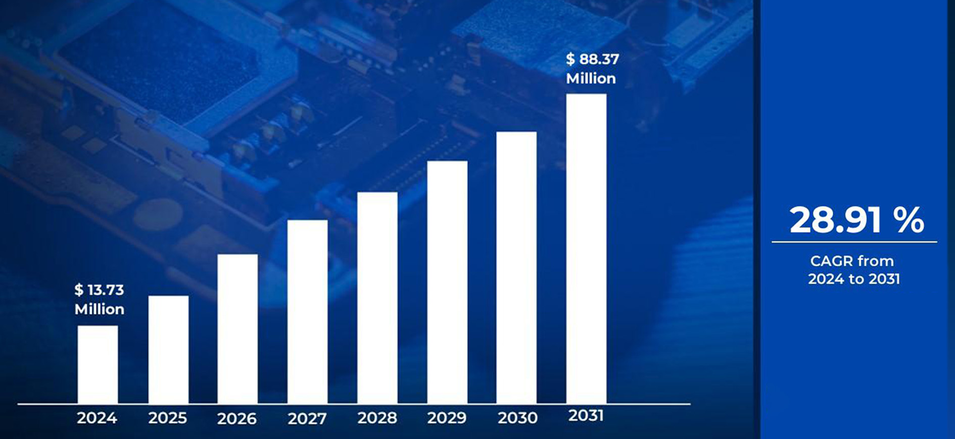
As the chart outlines, the Ga₂O₃ semiconductor advertise is anticipated to develop at an noteworthy Compound Yearly Development Rate (CAGR) of 28.91tween 2024 and 2031, coming to a advertise estimate of $88.37 million by 2031. This surge is fueled by the expanding request for high-power gadgets, energy-efficient hardware, and Ga₂O₃'s special capacity to function beneath extraordinary conditions.
The Future of Ga2O3
Research and Development
Ongoing research aims to resolve challenges such as p-type doping and improving crystal quality. Advancements in doping techniques, crystal growth, and fabrication methods will unlock new opportunities for Ga₂O₃ in various commercial applications. Once these hurdles are overcome, Ga₂O₃ could see widespread use in mainstream semiconductor devices.
Commercial Applications
As businesses like car, aviation, and renewable vitality look for more proficient high-power arrangements, Ga₂O₃ is well-positioned to ended up a key player. Its capacity to handle extraordinary conditions makes it perfect for high-voltage and high-temperature applications, and its advertise is anticipated to grow quickly as more businesses receive Ga₂O₃-based arrangements.
Conclusion
Ga2O3 is at the cutting edge of semiconductor innovation, opening modern conceivable outcomes with its ultra-wide bandgap and interesting properties. As investigate propels and challenges are tended to, Ga2O3 is set to ended up a key player within the semiconductor scene, especially in applications requiring tall effectiveness and performance.
Long term of Ga2O3 shows up shinning, with the potential to revolutionize different businesses and applications. As we proceed to investigate and open the riddles of Ga2O3, it holds the guarantee of transformative headways within the world of gadgets and past.
Commonly Asked Questions
What are the most applications of Ga2O3 semiconductors?
Ga2O3 is utilized in control contraptions, optoelectronics, high-temperature contraptions, and RF/microwave applications.How wide is the bandgap of Ga2O3, and why is it imperative?
Ga2O3 encompasses a bandgap of almost 4.8 eV, which permits for productive operation in high-temperature and high-voltage situations.What focal points does Ga2O3 have over GaN and SiC?
Ga2O3's 4.8 eV bandgap gives higher current thickness and voltage back compared to GaN (3.4 eV) and SiC (3.3 eV).What is the advertise viewpoint for Ga2O3?
The Ga2O3 advertise is anticipated to develop at a CAGR of 28.91% from 2024 to 2031, driven by demand for electric vehicles and renewable vitality.What are the most challenges for Ga2O3 semiconductors?
Key challenges include achieving p-type doping and managing material quality.Related Information

-

-
Phone
+86 135 3401 3447 -
Whatsapp