Cart ( )
Five steps to improve the electromagnetic compatibility of DC/DC switching power supplies
2024/5/14 11:29:49
Views:
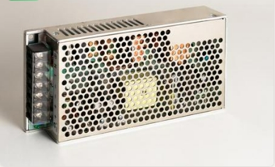
DC/DC switching power supply is indispensable in modern electronic products, and its high efficiency and small size are particularly important. However, switching devices in the design will bring about rapid voltage and current changes, making the product prone to problems during electromagnetic compatibility testing and prolonging the development cycle, especially in complex industrial environments.
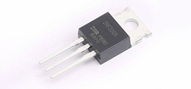
To deal with the electromagnetic compatibility problem of DC/DC switching power supply, it is first necessary to analyze the noise source and find the cause of excessive radiated and conducted emissions. In switching power supplies, switching frequency and its harmonics are the main sources of interference. Darkroom measurements will show a broadband interference spectrum from 30 MHz to 400 MHz. One of the reasons is the steep switching edge of the switching tube, such as the MOSFET output capacitance, junction capacitance, and the parasitic capacitance of the reverse recovery Schottky diode and the parasitic inductance of the traces. Together they result in a high frequency LC oscillation circuit.
Depending on the topology of the DC/DC switching power supply, the focus is also different. The BUCK circuit contains more high-frequency components due to the discontinuity of the input current, so the loop control and filter at the input are more critical. Due to the different key loops of the BOOST circuit, the focus should be on the output loop.
When designing a DC/DC switching power supply, the design of the input filter is crucial. The switching frequency of modern switching power supplies is usually between 250 kHz and 4 MHz, and LC filters are particularly suitable for controlling the fundamental wave and its higher harmonics. Typically, the filter's cutoff frequency is set to one-tenth the switching frequency. However, in practical applications, if the limit value is exceeded during electromagnetic compatibility testing, the cutoff frequency needs to be set lower to increase the suppression effect.
After adding a filter, sometimes the input terminal of the DC/DC switching power supply will oscillate. This is due to the negative input impedance and resonance caused by the LC filter circuit. The best way is to actively suppress the LC filter by adding an RC series circuit to reduce the resonant circuit factor Q value, thereby reducing the filter impedance.
In many cases, electrolytic capacitors with higher ESR are used instead, but be aware that ESR changes with frequency and temperature. The effect of frequency on ESR can be observed through Würth's REDEXPERT online platform. If you need to increase the effect of the filter at high frequencies, you can add magnetic beads, but you need to pay attention to the effect of current on the impedance of the magnetic beads.
There are also considerations when designing the output filter. To enhance the high-frequency suppression characteristics, a filter containing magnetic beads can be added to the output. Considering the impact of the DC resistance of the inductor and magnetic beads on the output current, the filter is placed in the feedback network of the DC/DC switching power supply to eliminate the impact of DC voltage drop.
However, filtering components within the feedback network may introduce undesirable phase shifts, affecting loop stability. A loop with a gain margin greater than 12dB and a phase margin greater than 45° can ensure stability. Loop compensation is the main measure, but it requires certain knowledge of automatic control theory and compensation circuit schemes.
As one of the key components of DC/DC switching power supply, inductor has a great impact on efficiency and cost. The REDEXPERT platform can quickly select the appropriate inductor and compare the AC and DC losses, temperature rise and other parameters of different devices. Ceramic capacitor MLCCs are widely favored due to their small size and low parasitic parameters. However, when using type II MLCCs, it is necessary to consider the effects of voltage bias and temperature.
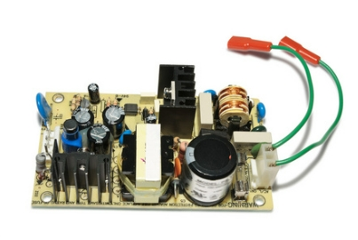
In order to reduce electromagnetic compatibility problems caused by DC/DC switching power supplies, it is crucial to reduce the loop area and ensure filter performance from the perspective of device layout and wiring. Key loop components should be placed together as much as possible to reduce the loop area. Ceramic capacitors for high-frequency filtering should be placed near the switch tube or IC, and the parasitic inductance can be reduced through short and thick traces. Reasonably connect the signal ground and power ground to avoid unnecessary antenna effects. Input and output filters should be arranged to eliminate capacitive and inductive coupling to the main parts of the circuit.
Through these design considerations, engineers can better design DC/DC switching power supplies that comply with electromagnetic compatibility.
To deal with the electromagnetic compatibility problem of DC/DC switching power supply, it is first necessary to analyze the noise source and find the cause of excessive radiated and conducted emissions. In switching power supplies, switching frequency and its harmonics are the main sources of interference. Darkroom measurements will show a broadband interference spectrum from 30 MHz to 400 MHz. One of the reasons is the steep switching edge of the switching tube, such as the MOSFET output capacitance, junction capacitance, and the parasitic capacitance of the reverse recovery Schottky diode and the parasitic inductance of the traces. Together they result in a high frequency LC oscillation circuit.
Depending on the topology of the DC/DC switching power supply, the focus is also different. The BUCK circuit contains more high-frequency components due to the discontinuity of the input current, so the loop control and filter at the input are more critical. Due to the different key loops of the BOOST circuit, the focus should be on the output loop.
When designing a DC/DC switching power supply, the design of the input filter is crucial. The switching frequency of modern switching power supplies is usually between 250 kHz and 4 MHz, and LC filters are particularly suitable for controlling the fundamental wave and its higher harmonics. Typically, the filter's cutoff frequency is set to one-tenth the switching frequency. However, in practical applications, if the limit value is exceeded during electromagnetic compatibility testing, the cutoff frequency needs to be set lower to increase the suppression effect.
After adding a filter, sometimes the input terminal of the DC/DC switching power supply will oscillate. This is due to the negative input impedance and resonance caused by the LC filter circuit. The best way is to actively suppress the LC filter by adding an RC series circuit to reduce the resonant circuit factor Q value, thereby reducing the filter impedance.
In many cases, electrolytic capacitors with higher ESR are used instead, but be aware that ESR changes with frequency and temperature. The effect of frequency on ESR can be observed through Würth's REDEXPERT online platform. If you need to increase the effect of the filter at high frequencies, you can add magnetic beads, but you need to pay attention to the effect of current on the impedance of the magnetic beads.
There are also considerations when designing the output filter. To enhance the high-frequency suppression characteristics, a filter containing magnetic beads can be added to the output. Considering the impact of the DC resistance of the inductor and magnetic beads on the output current, the filter is placed in the feedback network of the DC/DC switching power supply to eliminate the impact of DC voltage drop.
However, filtering components within the feedback network may introduce undesirable phase shifts, affecting loop stability. A loop with a gain margin greater than 12dB and a phase margin greater than 45° can ensure stability. Loop compensation is the main measure, but it requires certain knowledge of automatic control theory and compensation circuit schemes.
As one of the key components of DC/DC switching power supply, inductor has a great impact on efficiency and cost. The REDEXPERT platform can quickly select the appropriate inductor and compare the AC and DC losses, temperature rise and other parameters of different devices. Ceramic capacitor MLCCs are widely favored due to their small size and low parasitic parameters. However, when using type II MLCCs, it is necessary to consider the effects of voltage bias and temperature.
In order to reduce electromagnetic compatibility problems caused by DC/DC switching power supplies, it is crucial to reduce the loop area and ensure filter performance from the perspective of device layout and wiring. Key loop components should be placed together as much as possible to reduce the loop area. Ceramic capacitors for high-frequency filtering should be placed near the switch tube or IC, and the parasitic inductance can be reduced through short and thick traces. Reasonably connect the signal ground and power ground to avoid unnecessary antenna effects. Input and output filters should be arranged to eliminate capacitive and inductive coupling to the main parts of the circuit.
Through these design considerations, engineers can better design DC/DC switching power supplies that comply with electromagnetic compatibility.
Related Information
-

-
Phone
+86 135 3401 3447 -
Whatsapp