Cart ( )
Master Printed Circuit Assembly for Perfect PCB Circuit Boards
2023/4/15 17:29:43
Views:
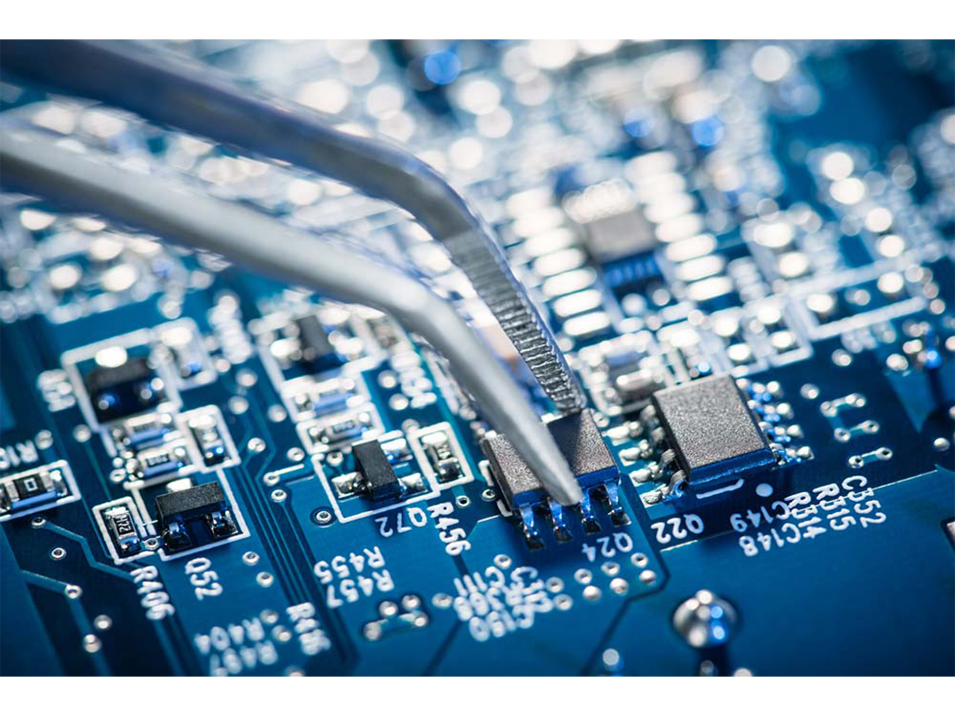
Printed circuit boards (PCBs) are the foundation of modern electronics. From smartphones to home appliances, almost every electronic device relies on a properly designed and assembled PCB. For engineers, hobbyists, and manufacturers, mastering printed circuit assembly is essential to achieving reliability and efficiency in electronic products.
What is a PCB?
Table of Contents
- The Basics of Printed Circuit Assembly (PCA)
- Steps in Printed Circuit Assembly
- Advanced Techniques in PCB Board Design
- Choosing the Right Manufacturer
- Common Mistakes in Circuit Board Layout
- Conclusion
- Commonly Asked Questions
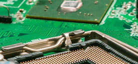
The Basics of Printed Circuit Assembly (PCA)
Printed circuit get together, commonly alluded to as PCA, includes mounting and interfacing components to a circuit board. This handle takes the uncovered PCB and changes it into a completely working electronic framework. Some time recently jumping more profound into get together procedures, let's characterize some key terms:
PCB (Printed Circuit Board)

PCBA (Printed Circuit Board Assembly)
The process of soldering and assembling components onto a PCB.
The successful completion of a PCA process involves several crucial steps, including soldering, inspection, and testing. These ensure that the components are correctly installed and function as intended.
Importance of Circuit Board Design in PCA
Compelling circuit board design is crucial to fruitful printed circuit get together. A well-structured plan diminishes the chance of fabricating blunders, guarantees flag judgment, and improves item toughness. Amid the plan stage, engineers ought to carefully consider component arrangement, follow directing, and warm administration. These factors significantly influence the performance of the final assembly.
Key Elements of Circuit Board Design
Steps in Printed Circuit Assembly
Presently that we have an understanding of the essentials, let's investigate the point by point steps included in printed circuit get together. Each stage is vital in guaranteeing the judgment and usefulness of the PCB printed circuit board.
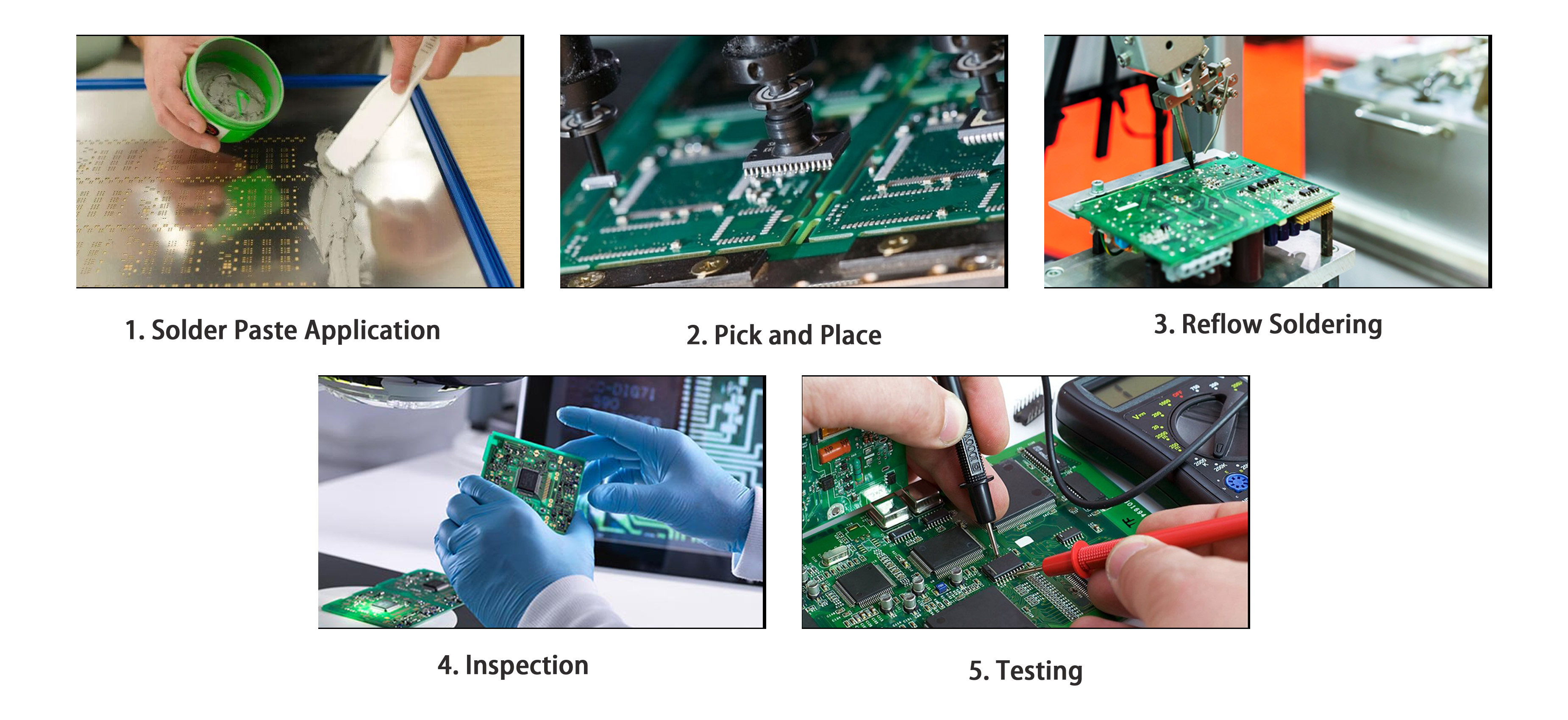
1. Solder Paste Application
The primary step in gathering a PCB board is applying patch glue to the fitting ranges where components will be mounted. This is often done employing a stencil that adjusts impeccably with the cushions on the board. Patch glue, a blend of modest patch balls and flux, guarantees that components can be joined safely.
2. Pick and Place
Once the patch glue is connected, components are put on the board. This step is either done physically for little amounts or through computerized pick-and-place machines for mass generation. Appropriate arrangement of components is basic for effective fastening.
3. Reflow Soldering
After putting the components, the board is warmed in a reflow broiler. This prepare dissolves the patch glue, shaping strong electrical associations between the components and the PCB. Legitimate temperature control is basic to avoid overheating or harming the components.
4. Inspection
Post-soldering, the PCB goes through an assessment stage. This step guarantees that all components are accurately mounted and patched without any abandons, such as shorts or open circuits. Computerized optical review (AOI) is commonly utilized to speed up this prepare in large-scale generation.
5. Testing
The last step within the get together handle is useful testing. Engineers perform different tests to confirm that the PCB works as intended. These tests may incorporate in-circuit testing (ICT), flying test tests, and utilitarian testing. Appropriate testing is basic to recognize potential disappointments some time recently shipping the item.
Advanced Techniques in PCB Board Design
High-Density Interconnect (HDI) Technology
As gadgets ended up littler and more capable, the require for high-density PCB plans increments. HDI sheets utilize better lines and littler vias, permitting for more components to be set in a littler space. This method upgrades flag judgment and diminishes electromagnetic obstructions.
Flexible Circuit Board Assembly
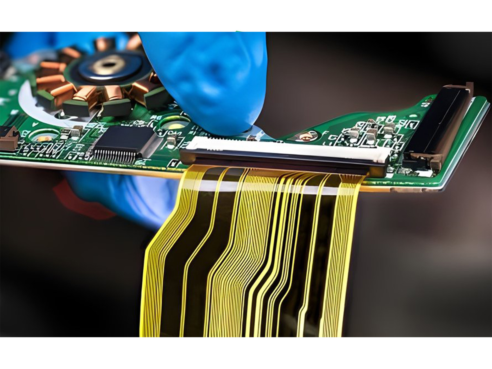
Flexible circuit boards, moreover known as flex PCBs, are utilized in applications where space and adaptability are basic. Gadgets like smartphones and wearables frequently utilize flexible circuit boards to diminish weight and spare space. Planning and amassing a flexible circuit board requires interesting contemplations, such as minimizing mechanical stretch choosing fitting materials that can withstand twisting.
Benefits of Flexible Circuit Boards
Choosing the Right Manufacturer
Selecting the proper producer for your PCB board plan is pivotal to guaranteeing a high-quality conclusion item. Not all producers are rise to, and variables such as fetched, innovation, and benefit quality can change essentially. Here are a few tips for choosing the leading printed circuit board producers:
1. Technology Capabilities
Ensure the manufacturer can handle the complexity of your design. For illustration, on the off chance that you're working on an HDI or flexible circuit board, you'll need a producer experienced in these zones.
2. Quality Assurance
Seek for producers that prioritize quality control. This incorporates certifications such as ISO 9001 and the capacity to perform exhaustive reviews and testing. High-quality control ensures your PCB will work as anticipated within the last item.
3. Cost Efficiency
In the event that you're searching for the cheapest PCB manufacturer, use caution not to give up quality for fetched. Whereas budget-friendly alternatives could appear engaging, the long-term costs of disappointments or absconds can be much higher. Balance affordability with reliability.
4. Lead Time
Consider how quickly a manufacturer can deliver your order. Lead times shift altogether depending on the complexity of the board, the manufacturer's capacity, and the topographical area. For time-sensitive ventures, guarantee the producer can meet your due dates.
Common Mistakes in Circuit Board Layout
Conclusion
Mastering printed circuit assembly requires attention to detail, from the initial circuit board layout to the final testing stage. By considering key components like circuit board design, warm administration, choosing the proper printed circuit board manufacturers, you'll be able guarantee your PCB board is solid and efficient. Whether you're working on a unbending or flexible circuit board, understanding the subtleties of the method will assist you create predominant electronic items.
Commonly Asked Questions
Why is "PCB" search volume high?
Growing demand for electronics across industries and increased interest from hobbyists boost searches.Which industries drive PCB search trends?
Consumer electronics, automotive, telecommunications, medical devices, and industrial automation.Impact of flexible and HDI PCBs on searches?
Rising use in compact devices like wearables and IoT increases interest in advanced PCB designs.Why interest in PCB manufacturing?
Companies seek affordable, quality PCB manufacturers, and hobbyists research prototyping options.How do environmental concerns affect PCB searches?
Interest in sustainable manufacturing and recycling drives searches related to eco-friendly PCBs.Related Information
-

-
Phone
+86 135 3401 3447 -
Whatsapp